Selecting materials for semiconductor fabrication requires uncompromising standards for purity, stability, and process compatibility.
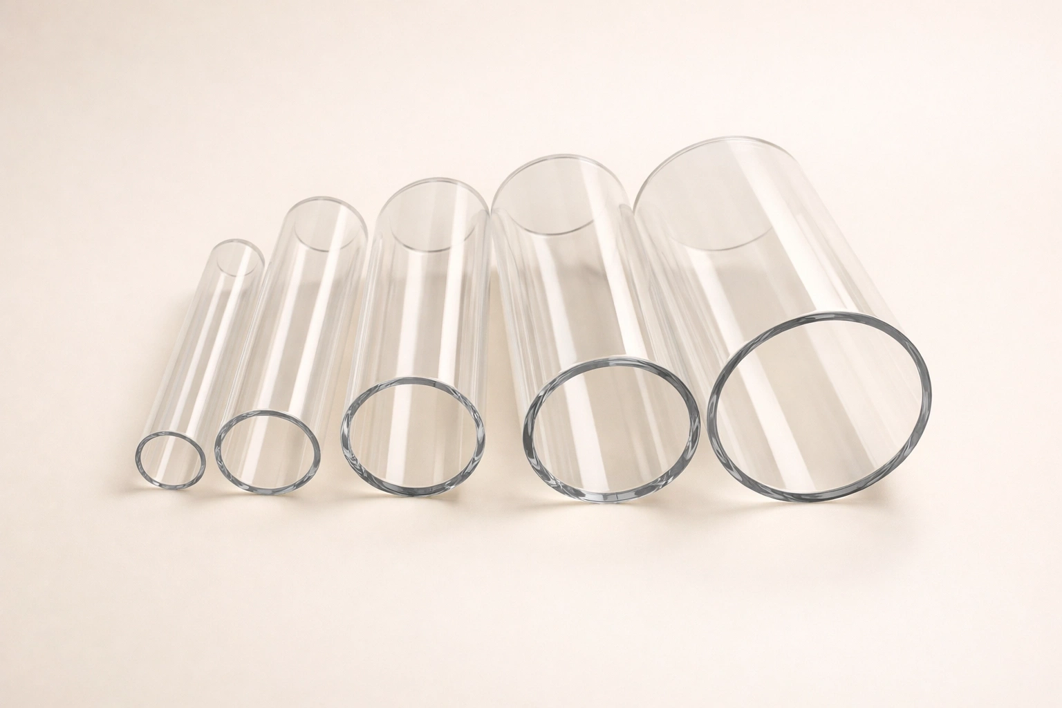
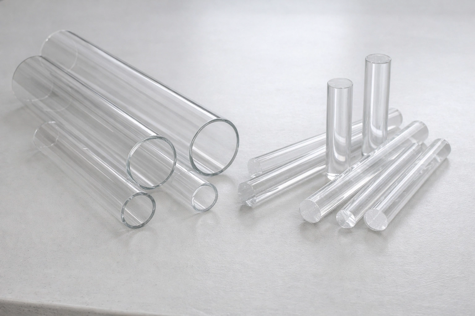
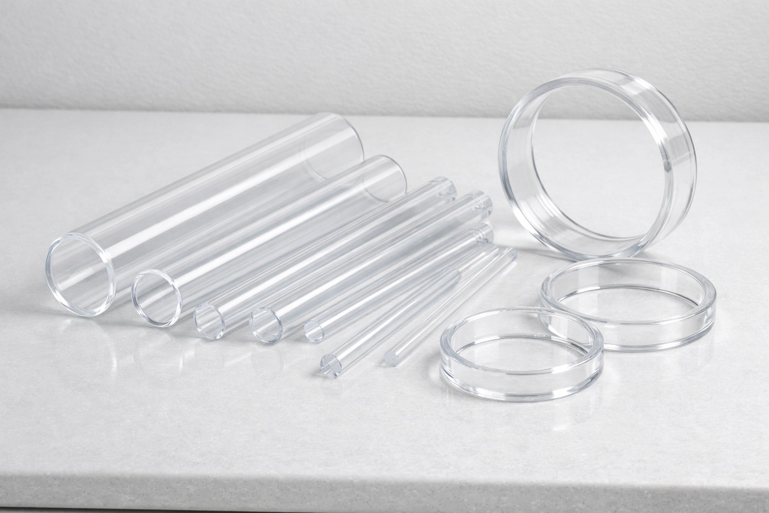
Quartz glass is essential for semiconductor manufacturing due to its ultra-high purity (>99.99% SiO₂), excellent thermal stability up to 1200°C, and superior plasma resistance. It enables critical processes including lithography, etching, deposition, and ion implantation by providing contamination-free environments and withstanding extreme process conditions that would degrade alternative materials.

From photomask substrates to plasma chamber liners, quartz glass underpins the reliability and yield of advanced semiconductor manufacturing. The following sections detail its unique properties, process-specific roles, and procurement best practices for fab environments.
What is Semiconductor-Grade Quartz Glass and Why is Ultra-Purity Critical?
Ensuring device yield and process reliability in semiconductor fabs demands materials with the lowest possible contamination risk.
Semiconductor-grade quartz glass, also known as high-purity fused silica, is a non-crystalline form of silicon dioxide refined to contain less than 1 ppm metallic impurities and minimal hydroxyl (OH) content. Ultra-purity is critical because even trace contaminants can introduce defects, reduce wafer yield, and compromise device performance at advanced process nodes.

Semiconductor-grade quartz is produced using flame hydrolysis or electric fusion of ultra-pure silica feedstock, followed by stringent cleaning and inspection protocols. The result is a material with exceptional chemical inertness, optical clarity, and resistance to devitrification, making it indispensable for contamination-sensitive fab processes.
Purity and Performance Metrics for Semiconductor Quartz
| Property | Type III Fused Silica | Type IV Fused Silica | Typical Requirement (Sub-10nm) |
|---|---|---|---|
| SiO₂ Content (%) | >99.95 | >99.995 | >99.995 |
| Metallic Impurities (ppm) | <10 | <1 | <1 |
| OH Content (ppm) | 10–200 | <1 | <1 |
| Particle Count (≥0.5μm/cm²) | <100 | <10 | <10 |
| UV Transmission (200–400nm) | 85–90% | >90% | >90% |
Why Do Advanced Fabs Depend on Fused Silica Components?
Maintaining process integrity in advanced fabs requires materials that can withstand harsh chemistries, high temperatures, and aggressive plasmas.
Fused silica components are favored in semiconductor fabs for their unmatched purity, low thermal expansion, and resistance to chemical and plasma-induced degradation. These properties are essential for minimizing contamination, ensuring dimensional stability, and extending component lifetimes in critical process tools.

Fabs rely on fused silica for wafer carriers, chamber liners, windows, and photomask substrates, where alternative materials would introduce unacceptable levels of contamination or fail under process conditions.
Key Advantages of Fused Silica in Fab Environments
| Attribute | Fused Silica Performance | Impact on Fab Processes |
|---|---|---|
| Ultra-High Purity | <1 ppm metallic impurities | Minimizes particle and ionic contamination |
| Thermal Stability | Up to 1200°C continuous use | Withstands rapid thermal cycling |
| Plasma Resistance | Excellent | Reduces erosion and particle shedding |
| Chemical Inertness | Excellent (except HF) | Compatible with acids, oxidizers |
| Low Thermal Expansion | 0.5 × 10⁻⁶/K | Maintains dimensional accuracy |
| Optical Clarity | >90% UV transmission | Enables photolithography, metrology |
Which Semiconductor Processes Require Quartz Glass Components?
Each stage of semiconductor fabrication presents unique material challenges that quartz glass is engineered to address.
Quartz glass is integral to processes such as lithography, plasma etching, CVD/ALD deposition, RTP/diffusion, and ion implantation. Its role varies from optical substrates to process chamber linings, ensuring both process purity and equipment longevity.


The following breakdown highlights the most critical applications and their technical requirements.
Quartz Glass Applications Across Semiconductor Processes
| Process Step | Quartz Component Examples | Key Requirements |
|---|---|---|
| Lithography | Photomask substrates, windows | UV transmission, flatness |
| Plasma Etching | Chamber liners, windows, rings | Plasma resistance, purity |
| CVD/ALD Deposition | Reactor tubes, boats, liners | High temp, chemical inertness |
| RTP/Diffusion | Furnace tubes, wafer carriers | Thermal shock resistance |
| Ion Implantation | Beamline windows, sample holders | Low contamination, durability |
Lithography and Photomask Systems
Lithography demands optical materials with exceptional UV transmission and surface flatness.
Quartz glass is used for photomask substrates and projection windows in deep ultraviolet (DUV) and extreme ultraviolet (EUV) lithography. Its high transmission (>90% at 193 nm) and low birefringence ensure precise pattern transfer and minimal image distortion.
Plasma Etching and Deposition Chambers
Plasma processes expose materials to energetic ions and reactive gases.
Quartz glass chamber liners, windows, and rings resist plasma erosion and prevent particle generation. Their ultra-high purity minimizes contamination, supporting high device yields in advanced etch and deposition tools.
How Does Quartz Glass Enable Advanced Lithography Systems?
Achieving nanometer-scale patterning requires optical materials with the highest transmission and dimensional stability.
Quartz glass enables advanced lithography by serving as the substrate for photomasks and as optical windows in exposure systems. Its low absorption at DUV wavelengths (193 nm, 248 nm) and minimal thermal expansion (<0.5 × 10⁻⁶/K) maintain focus and alignment during high-intensity exposure.

The use of high-purity fused silica reduces the risk of photomask defects and supports the production of sub-10nm features.
Lithography System Material Requirements
| Component | Material Specification | Performance Criteria |
|---|---|---|
| Photomask Substrate | Type IV fused silica | Flatness <0.1μm, OH <1ppm |
| Projection Window | Synthetic fused silica | >90% transmission at 193 nm |
| Reticle Carrier | High-purity quartz | Particle-free, dimensional stability |
What Role Does Fused Silica Play in Plasma Processing Equipment?
Plasma etching and deposition are among the most aggressive environments in semiconductor fabs.
Fused silica is used for chamber liners, windows, and focus rings due to its resistance to plasma-induced erosion and minimal particle generation. Its chemical inertness prevents reaction with process gases, while its low impurity content reduces the risk of device contamination.
The longevity of fused silica parts in plasma tools directly impacts tool uptime and wafer yield.
Fused Silica Performance in Plasma Environments
| Component | Plasma Exposure Type | Key Performance Metric | Typical Lifetime (cycles) |
|---|---|---|---|
| Chamber Liner | CF₄, SF₆, O₂ plasmas | Erosion rate <0.1 mm/1,000h | 5,000–10,000 |
| Window | UV/ion bombardment | Transmission loss <5%/1,000h | 2,000–5,000 |
| Focus Ring | Ion/radical exposure | Particle generation <10/cm² | 3,000–7,000 |
Why is Thermal Stability Critical for RTP and Diffusion Applications?
Rapid thermal processing (RTP) and diffusion require materials that can withstand extreme temperature gradients without cracking or deforming.
Quartz glass is ideal for RTP and diffusion furnace tubes, wafer carriers, and process boats due to its high softening point (1,730°C) and low thermal expansion. These properties enable rapid heating and cooling cycles (>100°C/s) while maintaining dimensional accuracy and preventing particle generation.
Thermal Performance Metrics for RTP/Diffusion
| Property | Quartz Glass Value | Impact on RTP/Diffusion |
|---|---|---|
| Max Continuous Temp (°C) | 1,050–1,200 | Supports high-temp annealing |
| Thermal Expansion (10⁻⁶/K) | 0.5 | Minimizes thermal stress |
| Thermal Shock Resistance | ΔT > 200°C | Withstands rapid cycling |
| Devitrification Rate | <0.01 mm/year | Maintains surface integrity |
How Do Ion Implantation Systems Benefit from Quartz Glass Properties?
Ion implantation exposes materials to high-energy ions and requires components with low contamination risk and high durability.
Quartz glass is used for beamline windows, sample holders, and end stations in ion implanters. Its ultra-high purity prevents metallic contamination, while its resistance to ion bombardment ensures long service life and minimal particle generation.
These properties are critical for maintaining device yield and preventing costly tool maintenance.
Quartz Glass in Ion Implantation
| Component | Exposure Type | Key Requirement | Typical Service Life (wafers) |
|---|---|---|---|
| Beamline Window | High-energy ions | No metallic contamination | 10,000–20,000 |
| Sample Holder | Ion/thermal exposure | Dimensional stability | 5,000–10,000 |
| End Station Liner | Plasma/ion exposure | Particle-free, durable | 8,000–15,000 |
What Purity Grades of Quartz Glass Match Different Process Nodes?
Matching quartz glass purity to process node requirements is critical for yield and device reliability.
Advanced nodes (<10nm) require Type IV fused silica with <1 ppm metallic impurities and OH content, while older nodes (>28nm) may tolerate Type III grades. The choice impacts both process yield and total cost of ownership.

Specifying the correct grade prevents costly yield loss and rework.
Quartz Glass Purity Selection Matrix
| Process Node (nm) | Recommended Quartz Grade | Metallic Impurities (ppm) | OH Content (ppm) | Typical Application Examples |
|---|---|---|---|---|
| <10 | Type IV | <1 | <1 | EUV lithography, advanced etch |
| 10–28 | Type III/IV | <10/<1 | <10/<1 | DUV lithography, CVD, RTP |
| 45–65 | Type III | <10 | <50 | Diffusion, ion implantation |
| >90 | Type II/III | <50/<10 | <200/<50 | Legacy tools, general labware |
What Technical Specifications Matter Most for Semiconductor Quartz Procurement?
Procurement for semiconductor fabs must focus on specifications that directly impact process yield and tool reliability.
Key technical specs include purity grade, OH content, particle count, dimensional tolerances, surface finish, and certification of compliance with industry standards. Custom fabrication capabilities and traceability are also critical for high-value applications.


A detailed specification sheet reduces the risk of quality issues and ensures compatibility with fab processes.
Semiconductor Quartz Procurement Specifications
| Specification | Typical Requirement | Impact on Fab Performance |
|---|---|---|
| Purity Grade | Type IV (>99.995% SiO₂) | Minimizes contamination |
| OH Content | <1 ppm | Prevents bubble/defect formation |
| Particle Count | <10/cm² (≥0.5μm) | Reduces yield loss |
| Dimensional Tolerance | ±0.05 mm or tighter | Ensures fit and alignment |
| Surface Finish | Ra < 0.5 μm | Minimizes particle generation |
| Certification | ISO/ASTM/SEMI compliant | Quality assurance |
| Traceability | Batch/lot number, COC | Enables root cause analysis |
How Do You Verify Quality Standards for Critical Fab Applications?
Quality verification is essential to prevent costly yield loss and tool downtime.
Verification protocols include incoming inspection (visual, dimensional, and surface analysis), particle count measurement, chemical analysis (ICP-MS for metallic impurities), and review of supplier certificates (COC, COA). For critical applications, third-party lab testing and on-site audits are recommended.

Documenting and archiving all test results supports traceability and continuous improvement.
Quality Verification Protocols
| Verification Step | Method/Tool | Acceptance Criteria |
|---|---|---|
| Visual Inspection | Microscope, UV lamp | No cracks, chips, inclusions |
| Dimensional Check | Caliper, CMM | Within specified tolerance |
| Surface Cleanliness | Particle counter, wipe test | <10 particles/cm² (≥0.5μm) |
| Chemical Purity | ICP-MS, FTIR | Metallic impurities <1 ppm |
| Certification Review | COC, COA, batch traceability | All documents present and valid |
Which Industry Certifications Apply to Semiconductor Quartz Components?
Compliance with recognized industry certifications ensures product quality and fab compatibility.
Key certifications include ISO 9001 (quality management), SEMI standards (e.g., SEMI PV, SEMI C79 for purity), ASTM E438 (laboratory glassware), and RoHS/REACH for hazardous substance control. These standards define requirements for purity, traceability, and process compatibility.

Specifying certified products reduces procurement risk and supports regulatory compliance.
Major Certifications for Semiconductor Quartz
| Certification/Standard | Scope/Industry | Key Requirements |
|---|---|---|
| ISO 9001 | All industries | Quality management system |
| SEMI PV/C79 | Semiconductor, solar | Purity, trace metals, documentation |
| ASTM E438 | Laboratory glassware | Chemical resistance, dimensional tolerances |
| RoHS/REACH | Electronics, EU market | Hazardous substance limits |
Decision Framework for Selecting Quartz Glass in Semiconductor Fabs
A systematic approach to material selection ensures optimal process performance and cost control.
The following checklist guides fab engineers and procurement teams through the critical decision points for specifying quartz glass in semiconductor applications.
Semiconductor Quartz Selection Checklist
| Step | Key Question | Recommended Action if "Yes" |
|---|---|---|
| 1 | Is the process node <28nm or yield-critical? | Specify Type IV fused silica, <1ppm OH |
| 2 | Will the part face plasma or aggressive chemistries? | Require plasma-grade, low-impurity quartz |
| 3 | Is UV/DUV/EUV transmission required? | Select synthetic fused silica, high clarity |
| 4 | Are rapid thermal cycles (>100°C/s) expected? | Prioritize low-expansion, high-purity quartz |
| 5 | Is traceability and certification mandatory? | Request full documentation and batch trace |
| 6 | Is lifecycle cost more important than upfront price? | Calculate ROI for higher purity grades |
Conclusion
Quartz glass is indispensable for semiconductor manufacturing, enabling contamination-free, high-yield processes across all advanced fab environments.
Selecting the right quartz glass for your fab is a critical engineering challenge. Leverage our factory-direct supply, engineering support, and acceptance of small-batch custom orders—backed by 20+ years of experience—to ensure your semiconductor processes meet the highest standards. Contact us for expert consultation and tailored solutions.
FAQ (Frequently Asked Questions)
What is the difference between Type III and Type IV fused silica for semiconductor use?
Type IV fused silica has lower metallic impurities (<1 ppm) and OH content (<1 ppm) than Type III, making it suitable for advanced nodes (<10nm) where contamination control is critical.
How can I verify the purity of quartz glass before installation in fab equipment?
Request ICP-MS chemical analysis reports, particle count certificates, and batch traceability documentation from your supplier. Third-party lab testing is recommended for critical applications.
What are the typical lead times for custom semiconductor quartz components?
Lead times vary by complexity and order volume; standard parts may ship in 3–5 days, while custom components typically require 3–5 weeks for fabrication and quality verification.
What procurement risks should I consider when sourcing quartz glass for semiconductor fabs?
Risks include insufficient purity, lack of certification, inadequate particle control, and unreliable supplier traceability. Always specify technical requirements and request supporting documentation.