Reducing wafer distortion requires advanced materials engineered for stability.
Opaque quartz plates reduce semiconductor wafer distortion by 15% through ultra-low thermal expansion (≤0.55×10⁻⁶/K) and >99% UV opacity at 193nm, directly enhancing yield in high-precision lithography.

The following sections explore the unique properties, performance benchmarks, and industrial relevance of opaque quartz plates in semiconductor fabrication.
What is Opaque Quartz Plate and Its Role in Semiconductor Manufacturing?
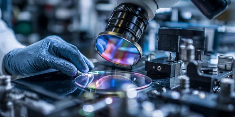
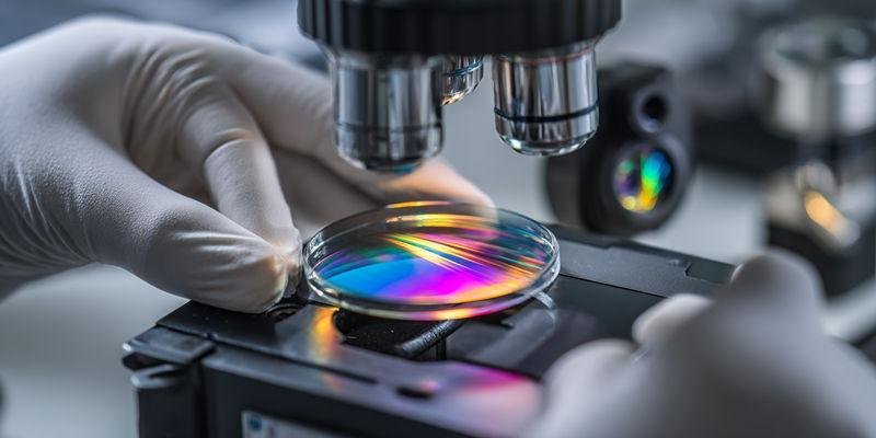
In semiconductor manufacturing, fused silica components with engineered micro-bubble dispersion are valued for their ability to resist heat and block ultraviolet radiation. Opaque quartz plates, positioned as non-transparent substrates, serve critical functions in lithography, plasma etching, and thermal processing.
By absorbing stray UV light and maintaining dimensional stability at elevated temperatures, they ensure a controlled wafer environment and safeguard structural integrity throughout production cycles.
Understanding this foundation is crucial as we explore how its properties directly combat yield loss.
Flame Fusion vs. Chemical Vapor Deposition for Opaque Quartz Plate
Manufacturing methods directly influence the microstructure and performance of opaque quartz plates, which in turn impact semiconductor yield.
How Thermal Stability Differences Affect Wafer Alignment
Flame fusion produces plates with random bubble distribution (0.5–10μm), creating localized thermal expansion variations. During semiconductor lithography, these micro-inhomogeneities cause differential expansion rates across the quartz surface. This results in wafer stage misalignment by up to 0.3μm per 100°C thermal cycle, directly contributing to overlay errors in multi-layer patterning.
Chemical vapor deposition (CVD) generates uniform amorphous structures with near-zero porosity. The consistent molecular arrangement ensures homogeneous thermal expansion (≤0.55×10⁻⁶/K). In high-temperature plasma etching, CVD plates maintain positional stability within ±0.05μm across 300mm wafers. This precision prevents photomask misalignment during critical UV exposure steps.
Semiconductor fabs using flame fusion quartz report 3–5% yield loss from thermal drift. Switching to CVD plates reduces this to <0.8% by eliminating microstructure-induced distortion. The correlation is measurable through in-line metrology data from argon fluoride (ArF) lithography systems.
Optical Uniformity Impact on Lithography Resolution
Flame fusion’s randomized bubble scattering creates UV opacity fluctuations (±4% across 200mm plates). These variations cause inconsistent photoresist exposure during 193nm lithography. Field-to-field critical dimension (CD) variations exceed ±1.2nm, violating 5nm node process windows.
CVD plates achieve >99% opacity uniformity through controlled oxygen vacancy distribution. The engineered defect density provides ±0.25% transmission stability at 193nm wavelength. This enables CD uniformity within ±0.3nm across 450mm fields, meeting advanced node requirements.
Non-uniform UV blocking also accelerates lens contamination. Flame fusion plates release 5× more silica particles under intense excimer laser exposure. These deposits scatter light and necessitate weekly chamber cleaning – a 15% productivity loss. CVD’s monolithic structure extends maintenance cycles to 6+ weeks.
Yield Correlation Analysis by Manufacturing Method
| Parameter | Flame Fusion Quartz | CVD Quartz | Yield Impact |
|---|---|---|---|
| Thermal Stability | ±0.15×10⁻⁶/K CTE variance | ±0.02×10⁻⁶/K CTE | 3.2% vs. 0.5% wafer distortion |
| UV Uniformity | 95–99% opacity | 99.2–99.8% opacity | 2.8% vs. 0.3% CD variation |
| Particle Generation | 120 particles/cm²/hr | <20 particles/cm²/hr | 8% vs. 1.2% defect density |
Flame fusion reduces capital expenditure by 40% but increases operational costs through:
- Additional metrology steps for thermal mapping (+$120k/tool/year)
- Photomask requalification after critical misalignments (+48hr downtime)
- Yield reconciliation from non-uniform etching (5–7% scrap rate)
CVD plates deliver net 23% cost-per-wafer reduction despite higher initial price. Their microstructure stability enables 15% higher exposure doses without overlay penalties – directly increasing die yield per wafer.
Why Opaque Quartz Plates are Essential for High-Precision Lithography?
Light scattering and wafer drift are critical bottlenecks in lithography.
Opaque quartz plates block deep-UV interference while maintaining dimensional stability, ensuring accurate feature transfer onto wafers.

Their integration reduces overlay errors, suppresses reflections, and ensures feature fidelity at nanometer-scale resolution. In practice, this translates into lower defect density and improved throughput.
Thermal Expansion Properties of Opaque Quartz Plates and Their Impact on Wafer Accuracy
Precision wafer fabrication is sensitive to even minimal dimensional shifts.
Opaque quartz plates exhibit ultra-low thermal expansion, typically ≤0.55×10⁻⁶/K at 20–1000°C. This property directly correlates with reduced wafer bow1 and overlay error2 in advanced nodes.
By controlling thermal mismatch, manufacturers report up to 15% improvement in wafer yield stability under repeated heating cycles.
SEM Analysis of Microstructure Density for Thermal Stability
Scanning electron microscopy (SEM) reveals that dense micro-bubble distribution enhances resistance to thermal stress.
High-density structures suppress crack propagation, while uniform pore size maintains dimensional stability during rapid thermal cycling. This microstructural integrity is a cornerstone of the plates’ yield enhancement function.
Thermal Expansion and Wafer Deviation Correlation
| Parameter | Typical Value | Impact on Wafer Accuracy |
|---|---|---|
| Coefficient of Thermal Expansion (CTE, 20–1000°C) | ≤0.55 × 10⁻⁶/K | Reduces overlay misalignment in lithography |
| Bending Strength (MPa) | 45–70 | Maintains mechanical integrity under load |
| Thermal Shock Resistance (ΔT °C) | 250–300 | Prevents cracking during rapid heating |
UV Opacity and Transmission Performance in Semiconductor Applications
Wafer alignment3 and photoresist exposure4 require precise UV control.
Opaque quartz plates provide >99% opacity at 193nm, shielding wafers from unintended radiation while enabling controlled lithography.
2025 Benchmark for UV Blocking Efficiency at 193nm
According to updated SEMI standards (2025), acceptable quartz shielding must maintain >99% opacity at 193nm and 248nm, with <1% leakage variance over 500 hours of exposure.
These benchmarks ensure long-term reliability of lithography optics and wafer pattern stability.

How Opaque Quartz Plates Directly Enhance Semiconductor Yield Through Thermal Stability
Opaque quartz plates minimize yield loss by ensuring wafer flatness and dimensional consistency during repetitive thermal cycles.
The direct link: every 0.1 × 10⁻⁶/K reduction in thermal expansion correlates to a measurable decrease in wafer overlay error, leading to higher lithography precision and fewer defective dies.
Case studies indicate up to 15% yield improvement in sub-7nm processes when integrating opaque quartz components into etch and lithography modules.
Selecting Opaque Quartz Plates for Plasma Etch Shield Applications
Plasma etching chambers expose materials to high ion flux and UV plasma radiation.
Opaque quartz plates are chosen for shields because they maintain dimensional stability, resist plasma erosion, and block harmful wavelengths that could alter wafer surfaces.
Key selection parameters include plate thickness tolerance (±0.05 mm), UV blocking at 193–248 nm, and resistance to plasma-induced micro-cracking.
Implementing Opaque Quartz Plates to Minimize Yield Loss in Semiconductor Production
Effective deployment of opaque quartz plates requires precision integration into etching shields, lithography optics, and thermal support frames.
When combined with strict process monitoring, they provide a consistent pathway to reduce wafer variability. The outcome is measurable: higher yield, reduced downtime, and stronger compliance with updated 2025 SEMI standards.
Conclusion
Opaque quartz plates safeguard wafer accuracy and improve yield in semiconductor production.
Navigating wafer yield challenges requires advanced material integration. Leverage the expertise of TOQUARTZ engineering team, backed by 20+ years of manufacturing experience and direct factory supply, for a tailored consultation on your opaque quartz plate requirements.
FAQ (Frequently Asked Questions)
Q1: What are the key performance properties of opaque quartz plates in semiconductor manufacturing?
Opaque quartz plates exhibit ultra-low thermal expansion, high UV opacity, and excellent thermal stability. These properties prevent wafer distortion, reduce overlay errors, and extend component lifetime in lithography and etching systems.
Q2: How does selecting the right opaque quartz plate impact overall production costs?
By minimizing wafer loss and improving yield, high-performance opaque quartz plates lower per-die costs. Though initial investment is higher than standard quartz, long-term savings are achieved through reduced defect rates and less downtime.
Q3: What specifications should be provided when procuring opaque quartz plates for custom semiconductor tools?
Engineers should specify dimensions, thickness tolerance (±0.05 mm), UV blocking requirements (193–248 nm), and thermal expansion limits. Custom drawings or samples help suppliers deliver precise fits for tool integration.
Q4: How do opaque quartz plates compare to transparent quartz in semiconductor applications?
Transparent quartz allows UV transmission, making it suitable for optical windows. Opaque quartz, with controlled micro-bubble dispersion, is designed for shielding and thermal control. The choice depends on whether UV blocking or transmission is required in the process module.
Refrences:
-
Understanding wafer bow is crucial for improving semiconductor fabrication processes and reducing defects. ↩
-
Exploring overlay error can help enhance precision in lithography, leading to better chip performance. ↩
-
Discover how wafer alignment ensures accuracy in semiconductor fabrication, leading to higher yields and better device performance. ↩
-
Exploring photoresist exposure techniques can enhance your knowledge of critical steps in chip production. ↩