- Home
- /
- Applications
- /
- Semiconductor Quartz Glass
- /
- Custom Process-Optimized Quartz Etching...


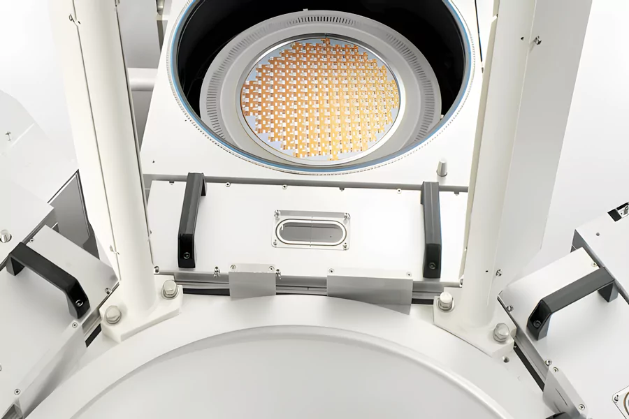
Custom Process-Optimized Quartz Etching Rings for Semiconductor Plasma Chambers-TOQUARTZ®
Features of Quartz Etching Ring
TOQUARTZ® semiconductor quartz rings are engineered specifically for plasma etching equipment, offering exceptional properties that ensure stable process conditions and extended service life in demanding semiconductor manufacturing environments.
Material Purity
Manufactured from premium grade quartz with 99.99% SiO₂ purity (up to 99.995% available), minimizing potential contamination in critical semiconductor processes.
Thermal Stability
Withstands extreme temperatures up to 1600°C with minimal thermal expansion (coefficient: 0.5×10⁻⁶/K), ensuring dimensional stability during thermal cycling in plasma etching processes.
Process Compatibility
Designed specifically for semiconductor etching processes including ICP, RIE, and DRIE systems, with optimized dimensions for various chamber configurations.
- Resists harsh semiconductor etchants
- Extremely low friction coefficient
- Ensures proper etch chamber sealing
Technical Specifications & Dimension of Quartz Etching Ring
TOQUARTZ® quartz etching rings are manufactured to precise specifications required for semiconductor processing equipment, featuring controlled physical, chemical, and thermal properties.
Technical Specifications of Quartz Etching Ring
| Property | Value | Notes |
| Material | High-Purity Quartz | 99.99% SiO₂ standard (up to 99.995% available) |
| Density | 2.2 g/cm³ | ±0.02 g/cm³ |
| Flexural Strength | 48 MPa | At room temperature |
| Elastic Modulus | 72 GPa | Young’s modulus |
| Poisson’s Ratio | 0.14-0.17 | – |
| Compressive Strength | 1100 MPa | At room temperature |
| Moh’s Hardness | 5.5-6.5 | – |
| Max Working Temperature (Long-term) | 1100°C | Continuous operation |
| Max Working Temperature (Short-term) | 1350°C | Intermittent exposure |
| Thermal Conductivity | 1.4 W/m·K | At 20°C |
| Thermal Expansion Coefficient | 5.5×10⁻⁷/°C | 20-1000°C range |
| Specific Resistance | 7×10⁷ Ω·cm | At 20°C |
| Surface Roughness | Ra≤0.8μm | Standard finish |
Size Chart of Fused Quartz Etching Ring
| Model | Specification | Outer Diameter (mm) | Thickness (mm) | Purity (%) |
| AT-TAZ-ER001 | 2-inch | 50.8 | 3 | 99.99 |
| AT-TAZ-ER002 | 4-inch | 101.6 | 4 | 99.99 |
TOQUARTZ® Solving Semiconductor Etching Challenges
with Quartz Rings
Quartz Etching Rings in High-Volume Semiconductor Fabs: Preventing Costly Production Line Downtime
Key Advantages
-
Scheduled Replacement Program Support
TOQUARTZ supports fixed-cycle delivery aligned with 3–6 month fab maintenance windows. -
Emergency Fulfillment in <48 Hours
Standard quartz etching rings can be shipped globally within 48 hours to prevent downtime. -
Batch Consistency Rate ≥ 99.7%
Dimensional and material consistency across batches ensures zero unplanned fitment failures.
TOQUARTZ® solution
A U.S.-based 12-inch DRAM fab operating 24/7 reported $220,000/day losses from unplanned etch ring failures.
TOQUARTZ® implemented a rolling 90-day replenishment plan and emergency stock buffer.
Within 6 months, downtime incidents dropped by 83%, and ring-related process interruptions were eliminated.
The fab now maintains a 99.9% uptime rate in its etch module with TOQUARTZ as its sole ring supplier.
Fused Quartz Etching Rings for Custom Equipment Manufacturers: Meeting Exact Dimensional Requirements
Key Advantages
-
±0.08mm Tolerance on OD/ID
TOQUARTZ achieves ±0.08mm tolerance on outer/inner diameters for OEM-specific chamber designs. -
Hole Position Accuracy ≤ ±0.1mm
Mounting holes are CNC-drilled with ≤ ±0.1mm positional deviation across 100mm span. -
Batch-to-Batch Deviation < 0.05mm
Dimensional deviation across batches is controlled under 0.05mm to ensure assembly repeatability.
TOQUARTZ® solution
A German OEM required 6-inch quartz rings with 6 asymmetric mounting holes and ±0.1mm tolerance.
Previous suppliers had a 12% rejection rate due to hole misalignment and edge chipping.
TOQUARTZ® delivered 300 rings with 0% rejection and <0.03mm deviation verified by CMM reports.
The OEM reduced assembly rework time by 40% and signed a 2-year supply agreement.
Quartz Glass Etching Rings for Advanced Process Development: Material Purity Requirements
Key Advantages
-
Metallic Impurity ≤ 10ppb
TOQUARTZ quartz rings are certified with ≤10ppb total metallic impurities for advanced node R&D. -
CF₄/O₂ Plasma Endurance ≥ 72h
Rings maintain structural integrity after 72-hour exposure to CF₄/O₂ plasma at 800°C. -
Surface Particle Count < 5 pcs/cm²
Post-cleaning particle count is controlled below 5 pcs/cm² (≥0.3μm) under ISO Class 5 conditions.
TOQUARTZ® solution
A Japanese R&D lab developing 3nm logic nodes required ultra-pure quartz rings for CF₄-based etching.
TOQUARTZ® supplied rings with ≤8ppb metal content and <3 pcs/cm² surface particles.
After 72h plasma exposure, no structural degradation or contamination was detected.
The lab reported a 92% reduction in particle-induced defects compared to previous suppliers.
TOQUARTZ® Customization Services for Quartz Etching Rings
Custom Design Capabilities
-
Dimensional Customization
Custom outer/inner diameters, thickness, and edge profiles tailored to your specific chamber design. -
Mounting Features
Precision-drilled mounting holes, slots, notches, or other features to ensure proper alignment and installation. -
Mounting Features
Precision-drilled mounting holes, slots, notches, or other features to ensure proper alignment and installation. -
Surface Treatments
Special surface finishes, including fire polishing, grinding, or chemical cleaning to meet specific surface roughness requirements.
Custom Order Process
-
Requirement Analysis
Submit drawings, specifications, or samples. Our engineers will review and discuss technical requirements. -
Design Confirmation
We provide detailed drawings for approval before production begins. -
Prototype Development
For complex designs, we can produce prototype samples for testing and validation. -
Production & Quality Control
Rigorous inspection and testing ensure all specifications are met. -
Delivery & Support
Fast shipping with complete documentation and technical support.
Usage & Maintenance Guidelines of Quartz Etching Ring
Proper handling, installation, and maintenance of quartz process rings are essential for maximizing performance and service life in semiconductor etching applications.
Handling & Installation
- Always handle quartz rings with powder-free cleanroom gloves to prevent contamination
- Inspect for chips, cracks, or surface defects before installation
- Ensure mounting surfaces are clean and free of particles
- Tighten mounting hardware gradually in a cross-pattern to ensure even pressure distribution
- Avoid over-tightening which can create stress points and lead to fractures
- Never use metal tools directly on quartz surfaces during installation
Maintenance & Replacement
- Establish a regular inspection schedule based on process conditions
- Monitor for signs of erosion, discoloration, or dimensional changes
- Typical replacement interval: 500-1000 process hours (varies by application)
- Develop a proactive replacement schedule to prevent unplanned downtime
- Clean using only approved semiconductor-grade solvents if necessary
- Avoid sudden temperature changes which can cause thermal shock
Storage Recommendations
- Store in original packaging until ready for use
- Maintain in a clean, dry environment with controlled humidity
- Ideal storage conditions: 20-25°C, 40-60% relative humidity
- Use soft, lint-free materials as separators between multiple rings
- Avoid stacking heavy items on top of quartz components
Need Quartz Etching Rings Technical Assistance?
Why Partner with TOQUARTZ
Direct Factory Advantage
As a direct manufacturer, we can cut out the numerous intermediate links.
Engineering Expertise
Technical team guides clients from material selection to design optimization, translating specs into deliverables.
Flexible Manufacturing
Handling standard & custom orders via small-batch expertise and prototyping rigor to meet urgent deadlines.
Quality
Assurance
Pre-shipment 3-step validation:
1. dimensional accuracy,
2. material purity ,
3. performance thresholds
Global Supply Chain
Reliable global logistics to industrial hubs (DE/US/JP/KR priority) with trackable milestones.
Releted Products
As a specialized manufacturer with direct factory capabilities, TOQUARTZ provides both standard and custom quartz solutions with engineering support throughout the specification and implementation process.
FAQ
Q: What is a quartz etching ring used for in semiconductor manufacturing?
A: Quartz etching rings (also called quartz process rings) are critical components in plasma etching equipment used in semiconductor manufacturing. They serve as spacers between the plasma chamber and the substrate being etched, helping to contain and direct the plasma, maintain process uniformity, and prevent contamination. Their high purity, thermal stability, and chemical resistance make them ideal for withstanding the aggressive plasma environments used in wafer etching processes.
Q: How does a quartz ring improve plasma etching processes?
A: Quartz rings improve plasma etching processes in several ways:
(1) They help maintain a consistent plasma environment by providing precise spacing and alignment within the chamber,
(2) Their high purity prevents metal contamination that could compromise semiconductor device performance,
(3) Their thermal stability ensures dimensional consistency during temperature fluctuations;
(4) Their electrical insulating properties help control plasma distribution.
These benefits collectively contribute to improved etching uniformity, higher process yields, and more consistent device performance.
Q: What are the material requirements for quartz rings in semiconductor etching?
A: Quartz rings for semiconductor etching must meet strict material requirements:
(1) High purity (typically 99.99% SiO₂ or higher) to prevent contamination,
(2) Excellent thermal stability to withstand process temperatures up to 1600°C,
(3) Superior chemical resistance against corrosive gases and plasma,
(4) Low thermal expansion coefficient for dimensional stability,
(5) Consistent material properties with minimal defects or inclusions,
(6) Precise dimensional tolerances, typically ±0.1mm or better.
These requirements ensure process reliability and prevent yield losses in wafer fabrication.
Q: Are your quartz rings compatible with fluorine-based etching processes?
A: Yes, our quartz etching rings are compatible with fluorine-based etching processes commonly used in semiconductor manufacturing. Our high-purity quartz formulation provides excellent resistance to fluorinated gases such as CF₄, SF₆, NF₃, and CHF₃. While all quartz will experience some gradual erosion in fluorine plasma environments, TOQUARTZ rings demonstrate superior durability with erosion rates typically 20-30% lower than standard commercial quartz. For particularly aggressive fluorine processes, we can recommend optimized compositions and thicknesses to maximize service life.
Q: How do quartz etching rings compare to ceramic alternatives?
A: Quartz etching rings and ceramic alternatives (typically alumina or aluminum nitride) each have distinct advantages: Quartz offers superior purity (99.99%+ SiO₂), excellent transparency for optical monitoring, lower particle generation, and very low thermal expansion. Ceramics typically provide better mechanical strength, higher thermal conductivity, and in some cases better resistance to specific plasma chemistries. The choice depends on process requirements – quartz is generally preferred for applications requiring high purity, optical clarity, and minimal thermal expansion, while ceramics may be selected for applications requiring greater structural strength or thermal management.
Contact our engineering team for technical consultation and pricing. We’ll help you select the optimal specifications for your application requirements.