Hassas optik sistemler, tasarım hatasından değil, malzeme uyumsuzluğundan dolayı arızalanır. Standart alt tabakalar geometrik veya spektral gereksinimleri karşılayamadığında, performans kaybı kaçınılmazdır.
Erişmiş silika alt tabakaları, optik ve endüstriyel ölçüm cihazlarında kritik bir öneme sahiptir; ancak katalog standart formatları ile boyutsal olarak özel olarak tasarlanmış çözümler arasında seçim yapmak nadiren kolaydır. Bu makale, boyutsal toleranslar, kaplama uyumluluğu, uygulamaya özgü gereksinimler ve ölçülebilir optik performans açısından kapsamlı bir teknik karşılaştırma sunarak, mühendislere ve sistem entegratörlerine belirli bir optik montaj için hazır stok ürünlerinin mi yoksa amaca özel üretimin mi uygun yol olduğunu değerlendirmeleri için gerekli parametrik temeli sağlar.
Bu karşılaştırma, yerleşik optik üretim standartlarına, malzeme karakterizasyon verilerine ve UV, görünür ışık ile yakın kızılötesi dalga boyu aralıklarında belgelenmiş performans davranışlarına dayanmaktadır. Her bölüm, bu kararın farklı bir teknik boyutunu ele almakta ve tüm analitik çerçeveyi uygulamaya yönelik bir formatta bir araya getiren pratik bir ön şartname kontrol listesiyle son bulmaktadır.
Standart Erimiş Silika Levhaların Optik ve Boyutsal Sınırları
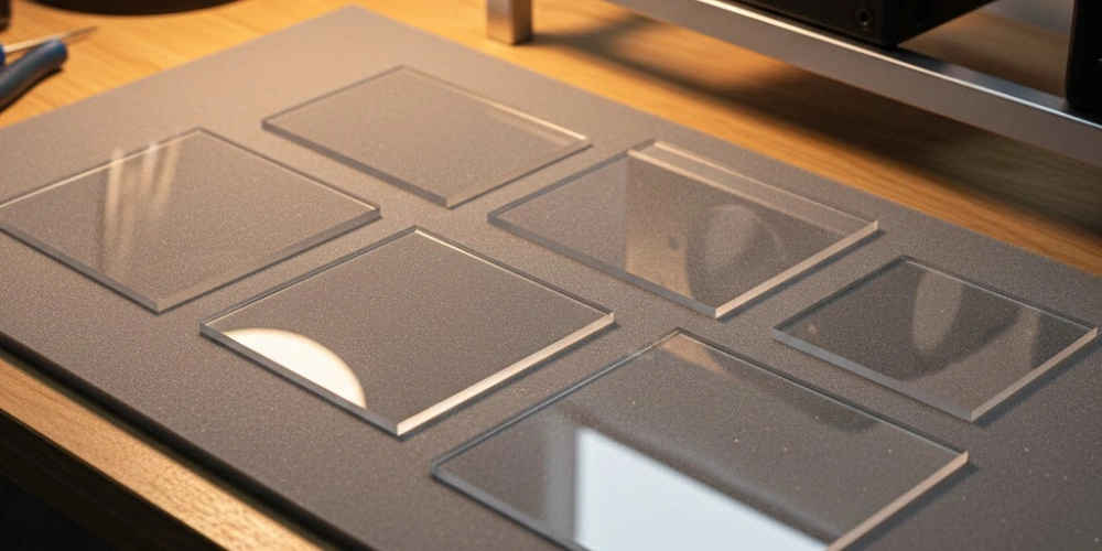
Standart katalogdaki erimiş silika plakalar, tüm uygulamaya özgü sapmaların ölçülmesi gereken referans noktasını oluşturur. Bu referans noktasının tam olarak nerede bittiğini belirlemek, mantıklı bir alt tabaka seçim sürecinin ön koşuludur.
Piyasada bulunan erimiş silika plakalar, genellikle 10 mm ile 150 mm arasındaki dairesel çaplarda ve 10 × 10 mm ile 100 × 100 mm arasındaki dikdörtgen boyutlarda olmak üzere, belirli boyut gruplarında üretilmektedir. Kalınlık seçenekleri de benzer şekilde belirli aralıklarla sunulur; yaygın değerler 0,5 mm, 1 mm, 2 mm, 3 mm ve 5 mm'dir. Standart katalog ürünlerinin yüzey kalitesi genellikle MIL-PRF-13830B standardına göre 60-40 çizik-çukur olarak belirtilir ve 632,8 nm'de yüzey düzlüğü λ/4 ile λ/10 aralığındadır. Stokta bulunan ürünlerin paralellik toleransları genellikle 1 ile 5 ark dakikası arasındadır ve çap veya kenar toleransları, tedarikçi kademesine bağlı olarak ±0,1 mm ile ±0,25 mm arasında tutulur.
Bu sınırlar keyfi değildir — bunlar, sabit bir parametre alanı içinde tekrarlanabilir çıktı elde etmek amacıyla parlatma döngülerinin, denetim veriminin ve hammadde kullanımının optimize edildiği yüksek hacimli üretimin ekonomik gerçeklerini yansıtır. Bu alan içinde, standart plakalar güvenilir bir şekilde çalışır. Bu alanın dışında ise performans varsayımları hızla çöker ve optimal olmayan bir standart alt tabakanın kullanılması, sistem düzeyinde entegrasyon bunları ortaya çıkarana kadar genellikle görünmez olan sistemik hata kaynaklarına yol açar.
Standart sınıf erimiş silikanın kırılma indisi homojenliği, genellikle açık açıklık boyunca Δn < 5 × 10⁻⁵ olarak belirtilir. Düşük koheranslı veya geniş bant görüntüleme uygulamaları için bu değer genellikle yeterlidir. Ancak, dalga cephesi hata bütçelerinin milidalga cinsinden ölçüldüğü interferometrik, holografik veya dar çizgi genişliğine sahip lazer uygulamaları için, bu düzeydeki hacimsel homojen olmama durumu bile toplam sistem dalga cephesi hatasına göz ardı edilemeyecek bir katkı sağlar. Standart katalog ürünleri, partiye özgü kırılma indisi homojenliği sertifikası sunmaz; bu da mühendisin, bu belirsizliği sınırlayacak ampirik veriler olmadan sistem hata bütçelerine dahil etmesi gerektiği anlamına gelir.
Standart Erimiş Silika Plakaların Hassas Sistemlerde Yetersiz Kaldığı Noktalar
Hassas optik sistemlerdeki boyutsal ve spektral kısıtlamalar, genellikle katalogda bulunan ürün yelpazesinin karşılayabileceğinin ötesine geçer. Standart alt tabakaların yapısal sınırlamaları, malzeme yetersizliğinden değil, sabit formatlı üretimin doğasında var olan esneksizlikten kaynaklanır — ve bu sınırlamaların nerede devreye girdiğini anlamak, sıkı optik performans bütçeleri dahilinde çalışan her sistem mimarı için hayati önem taşır.
Boyutsal Esneksizlik ve Montaj Toleransı Çatışmaları
Mekanik muhafazalara, vakum flanşlarına veya çok eksenli montaj parçalarına entegre edilen optik alt gruplar, tamamen mekanik tasarım tarafından belirlenen geometrik sınır koşulları getirir — bu koşullar, alt tabaka kataloglarında ticari olarak bulunan ürünlere göre belirlenmez.
Standart dairesel erimiş silika plakalar, genellikle ±0,1 mm ile ±0,25 mm arasında bir dış çap toleransına sahiptir.; bu da tüm aralık boyunca en fazla 0,5 mm’lik bir çap farkına karşılık gelir. O-ring ile sızdırmazlığı sağlanan ve oluk çapı ±0,05 mm hassasiyetinde işlenmiş bir vakum gözetleme penceresinde, bu uyumsuzluk ya eksik sızdırmazlığa ya da mekanik çakışmaya neden olur; bu durumların hiçbiri, optik veya muhafazanın yeniden imal edilmeden düzeltilemez. Uygulamada, muhafaza neredeyse hiçbir zaman yeniden işlenmez; bu da optiğin değiştirilmesi gerektiği anlamına gelir. Dahası, Standart plakalar için genellikle 1–5 yay dakikası olarak belirtilen paralellik toleransları, doğrudan açısal ışın sapmasına karşılık gelir her ışın geçirgen yüzeyde — 3 mm kalınlığında ve 3 ark-dakika paralellik hatası olan bir plaka için, iletilen ışın yayılma mesafesinin her metresi başına yaklaşık 2,6 µm yan yönde sapma gösterir; bu hata, katlanmış veya çok geçişli rezonatör tasarımlarında kritik düzeyde birikir.
Sonuç olarak, kinematik bir montaj parçası, kriyojenik pencere yuvası veya ultra yüksek vakumlu flanş gibi herhangi bir hassas mekanik arayüz, üreticinin standart üretim serisinden devralınan toleranslara değil, mekanik çizimdeki toleranslara uygun olarak imal edilmiş alt tabakalara ihtiyaç duyar.
Sabit Biçimli Alt Tabakalarda Kaplama Bölgesi Kısıtlamaları
Standart formatlı alt tabakalara uygulanan yansıma önleyici, yüksek yansıma ve ışın bölücü kaplamalar, alt tabakanın geometrisi sabitlendikten sonra kaplanır; bu da, kaplama alanının standart plakanın sağladığı açıklıkla sınırlı olduğu anlamına gelir — bu açıklığın, amaçlanan uygulamadaki optik ışın iziyle hizalı olup olmadığına bakılmaksızın.
Eksen dışı veya asimetrik optik sistemlerde, alt tabaka üzerindeki ışın izi ne merkezde ne de daireseldirve standart bir plakanın kullanılabilir kaplamalı alanı, bir eksende işlevsel ışın bölgesinin önemli ölçüde ötesine uzanırken, diğer eksende bu bölgeye yetmeyebilir. Bu durum, kaplamalı iletim için etkili açık açıklığın azalmasına ve ışın marjının — ışının kenarı ile kaplanmış bölgenin kenarı arasındaki mesafe — kaplama kenarı saçılma artefaktlarını önlemek için tipik olarak gerekli olan minimum 2 mm'lik tampon mesafesini karşılamamasına neden olur. Kaplama kenarlarından kaynaklanan saçılma katkılarının, tepe yoğunluğunun 10⁻³ ila 10⁻⁴ altında seviyelerde parazit ışık oluşturduğu ölçülmüştür, bu durum arka plan bastırmanın performansın temel belirleyicisi olduğu floresan algılama, Raman spektroskopisi ve düşük sinyalli interferometri gibi uygulamalarda olumsuz etki yaratmaktadır.
Ayrıca, gezegensel dönüşlü kaplama sistemlerindeki biriktirme geometrisi, alt tabakanın tüm çapı boyunca film homojenliğini optimize eder. Standart formatlı bir alt tabaka, çok elemanlı bir düzende eğik bir açıyla veya yanal olarak kaydırılmış bir konumda kullanıldığında, işlevsel ışın bölgesi boyunca kaplama homojenliği teknik özelliklerden sapabilir ve bu da tüm optik zincir boyunca yayılan, dalga boyuna bağlı iletim homojenliği bozukluğuna yol açabilir.
Dairesel Olmayan ve Düzensiz Açıklık Gereksinimleri
Optik ve optoelektronik sistemlerin önemli bir kısmı, hiçbir standart ürün kataloğunda yer almayan açıklık geometrilerine ihtiyaç duyar — dikdörtgen yarıklar, eliptik pencereler, çokgen açıklıklar ve hassas işlenmiş deliklere veya alt tabakaya entegre edilmiş montaj özelliklerine sahip plakalar.
Özellikle spektral cihazlar, optik kataloglarındaki standartlardan ziyade, dedektör dizisinin geometrisine bağlı olarak belirlenen açıklık şekillerini gerektirir. Doğrusal bir CCD veya InGaAs dizi dedektörü, 3 mm × 40 mm net açıklığa sahip bir erimiş silika giriş penceresine ihtiyaç duyabilir — bu boyut, dizi kenarlarında vinyetleme oluşmasına yol açmadan hiçbir standart dairesel veya kare plaka ile yaklaştırılamaz. Benzer şekilde, Plazma aşındırma ve kimyasal buhar biriktirme ekipmanlarındaki çok portlu vakum odaları, standart dışı dış profillere sahip gözetleme pencerelerine ihtiyaç duyar standart optik çaplara uymayan birleştirilmiş flanş konfigürasyonlarıyla eşleştirilmek üzere. Belgelenmiş yarı iletken işleme ekipmanı konfigürasyonlarında, özel kuvars plakalar Sistem entegrasyon denetimleri sırasında incelenen görüntü penceresi spesifikasyonlarının %’sini aşan bir oranda, asimetrik flanş geometrilerine sahip ürünler talep edilmektedir.
Bu geometrilerin imalatı, cilalı alt tabakanın CNC su jeti veya lazerle şekillendirilmesini ve ardından kenar işleme işlemlerini gerektirir; bu işlemler, tanımı gereği standart katalog üretiminden hariç tutulur ve yalnızca özel imalat iş akışları yoluyla gerçekleştirilebilir.
Kalınlık Kısıtlamaları ve Bunların Dalga Cephesi Hatasına Etkisi
Standart erimiş silika kataloglarında yer alan ayrık kalınlık değerleri, alt tabaka kalınlığının performansı belirleyen bir değişken olduğu her türlü sistemde — dispersif elemanlar, etalon bileşenleri ve koheransa duyarlı geçirgenlik pencereleri dahil — nicel bir tasarım kısıtlaması getirmektedir.
Normal ışınlama durumunda, kırılma indisi n ve kalınlığı t olan düzlem-paralel bir plakanın yarattığı optik yol farkı (OPD), şu formülle verilir: OPD = (n – 1) × t, ve 589 nm dalga boyunda n = 1,4584 olan erimiş silika için, tasarımda belirlenen optimum değerden 1 mm’lik bir kalınlık sapması, 0,458 mm’lik bir OPD kaymasına neden olur — bu değer, çoğu dar bantlı lazer kaynağının koherans uzunluğunu çok aşmaktadır. Şu durumda Fabry-Pérot etalonu1 konfigürasyonlar; burada serbest spektral aralık, FSR = c / (2 × n × t) formülüyle belirlenir, 3 mm’lik bir erimiş silika etalonda ±0,1 mm’lik bir kalınlık hatası, 1550 nm’de FSR’yi yaklaşık 1,6% kadar kaydırır — Yoğun dalga boyu bölmeli çoklama uygulamalarında, iletim tepe değerlerini hedef ITU kanal bant genişliğinin dışına kaydırmaya yetecek bir hata. 3 mm'lik standart katalog ürünleri, bu tür konfigürasyonlar için tipik olarak gerekli olan ±0,02 mm'lik kalınlık toleransını garanti edemez; zira bu ürünlerin kalınlık toleransları ±0,1 mm ile ±0,2 mm arasında belirtilmiştir — bu da etalon sınıfı gereksinimlere kıyasla beş ila on kat daha düşük bir değerdir.
Hazır Ürünler Yerine Özel Üretim Kuvars Plakaların Tercih Edilmesi Gereken Durumlar
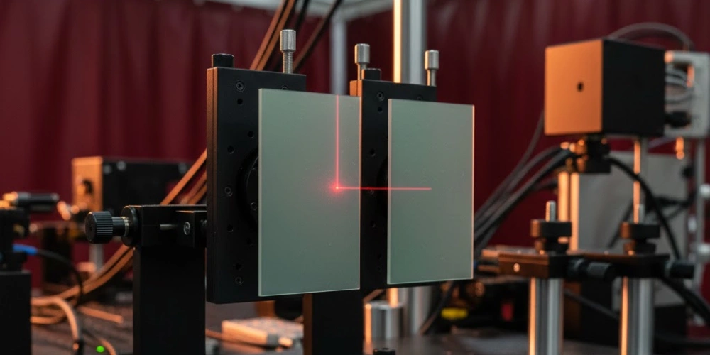
Boyutsal ve kaplama sınırlamalarının ötesinde, bazı uygulama ortamları o kadar spesifik sistem düzeyinde kısıtlamalar getirir ki, hiçbir katalog ürünü yapısal olarak bu kısıtlamaları karşılayamaz. Bu senaryolar, amaca özel olarak tasarlanmış alt tabakalar lehine en net teknik argümanı oluşturur ve yarı iletken işleme, lazer sistemi entegrasyonu, spektroskopik cihazlar ve havacılık-uzay optik yükleri alanlarında belgelenmiş bir düzenlilikle ortaya çıkar.
Yarı İletken ve İnce Film Biriktirme Ekipmanlarındaki Vakum Odası Pencereleri
Fiziksel buhar biriktirme ve kimyasal buhar biriktirme odaları, 10⁻³ ile 10⁻⁹ Torr arasındaki basınç aralıklarında çalışır; bu durum, gözetleme pencereleri için sızdırmazlık gereklilikleri getirir ve bu gereklilikler tamamen flanş geometrisine ve monte edilen malzemenin gaz salınımı özelliklerine göre belirlenir.
Oda sıcaklığında 24 saatlik pompalama işleminin ardından, erimiş silikanın gaz salınım hızları yaklaşık 10⁻¹⁰ Torr·L·s⁻¹·cm⁻² olarak ölçülmüştür., bu da onu mevcut en düşük gaz salınımlı optik malzemeler arasında yer almasını ve UHV uyumlu gözetleme penceresi imalatı için tercih edilen bir seçenek haline getirir. Ancak, UHV uyumluluğunun sağlanması yalnızca bir malzeme özelliği değildir — bunun için ayrıca alt tabaka geometrisinin sızdırmazlık oluğu boyutlarıyla ±0,05 mm hassasiyetinde eşleşmesi, kenar profilinin sızdırmazlık temas noktasında gerilim yoğunlaşmasını önlemek için pahlı olması ve metal veya elastomer sızdırmazlık elemanının uyumunu sağlamak için sızdırmazlık bölgesi içindeki yüzeyin λ/4 veya daha iyi bir düzlük spesifikasyonunu karşılaması gerekir. Hiçbir standart katalog plakası, bu geometrik ve yüzey spesifikasyonlarını tek bir üründe bir araya getirmez.
Oda yeterlilik değerlendirmesi sırasında incelenen, belgelenmiş proses ekipmanı konfigürasyonlarında, dış çap toleransı ±0,025 mm ve paralellik değeri 30 yay saniyenin altında olan özel kuvars plakalar gerekliydi Değerlendirilen 70%'den fazla görüntüleme alanı konumunda. Alternatif çözüm — sızdırmazlık uyumluluğunu sağlamak için standart bir plakanın altlık ile desteklenmesi — altlık arayüzünde partikül kirliliği riski doğurdu; bu durum, 10 nm altındaki işlem düğümü temizlik gereklilikleriyle bağdaşmayan bir sonuçtu.
Lazer Sistemlerinde Entegre Optik Yol Bileşenleri
Endüstriyel kesim platformları, bilimsel Ti:Safir osilatörleri ve darbeli Nd:YAG konfigürasyonları dahil olmak üzere yüksek güçlü lazer sistemlerinde, ışın yönlendirme alt tabakaları, kısmi yansıtıcılar ve çıkış kuplörü tabanları olarak erimiş silika plakalar kullanılır; bu uygulamalarda, alt tabakanın rezonatörün optik yol uzunluğuna katkısının kesin olarak belirtilmesi gerekir.
Normal ışın açısında bir erimiş silika plakanın optik yol uzunluğuna katkısı OPL = n × t'dirve ±10 fs² düzeyinde grup gecikme dağılımı (GDD) yönetimi gerektiren 800 nm’lik bir femtosaniye osilatör boşluğu için, erimiş silika substratındaki 0,1 mm’lik bir kalınlık hatası bile yaklaşık 3,5 fs²’lik bir GDD sapmasına yol açar, bu da tek bir bileşende toplam GDD bütçesinin 35%'sini tüketir. Bu nedenle, ±0,02 mm kalınlık toleranslarına göre imal edilen özel kuvars plakalar, bir performans lüksü değil, boşluk stabilitesi için bir gerekliliktir. ultra kısa darbeli sistemlerde. Ayrıca, 1 mJ’nin üzerindeki darbe enerjilerinde ve 1 kHz’yi aşan tekrarlama frekanslarında, ışın şekillendirme optiklerinin etkisiyle alt tabaka üzerindeki ışın izi genellikle dairesel simetriden sapar; bu durum, standart stokta bulunan dairesel formatlar yerine, gerçek ışın profiline uygun alt tabaka açıklıklarının kullanılmasını gerektirir.
Hassas kalınlık kontrolü, uyumlu açıklık geometrisi ve lazer hasarına dayanıklı yüzey kalitesinin (yüksek güçlü uygulamalar için tipik olarak 10⁻⁵ çizik-çukur) bir araya gelmesi, ancak her bir spesifikasyonun bağımsız olarak ele alındığı ve sistem tasarımına göre doğrulandığı özel üretim iş akışları yoluyla sağlanabilir.
Spektroskopik Cihazlar için Özel Diyafram Yapılandırmaları
Spektroskopik cihazlar — ızgara spektrometreleri, Fourier dönüşümlü kızılötesi sistemler ve rezonatörle güçlendirilmiş absorpsiyon spektrometreleri dahil — dispersif elemanın geometrisi, dedektör dizisi biçimi ve toplama optiğinin uzamsal koherans gereksinimleri tarafından belirlenen açıklık sınır koşullarını dayatır.
512 elemanlı doğrusal bir InGaAs dedektör ile 200–2500 nm aralığını kapsayan tipik bir ızgara spektrometre tasarımında, giriş penceresinin net açıklığı 4 mm × 38 mm olarak belirtilmiştir. — kenarları cilalanmış ve tüm net açıklık boyunca λ/10 yüzey düzgünlüğüne sahip özel dikdörtgen erimiş silika alt tabakalar gerektiren bir format. 38 mm boyut, 25 mm × 25 mm’lik standart kare formatı 52% kadar aşmaktadır; bu da, hiçbir standart katalog ürününün gerekli vinyetlenmemiş açıklığı sağlayamayacağı anlamına gelir. Ayrıca, Kaydedilen spektrumda yapay yoğunluk gradyanlarının oluşmasını önlemek için, 38 mm boyutundaki iletimin uzamsal homojenliği ±0,5% aralığında tutulmalıdır — sadece standart küçük formatlı bir plakanın kapladığı merkezi bölgeyi değil, alt tabakanın tamamı üzerinde kontrollü bir parlatma işlemini gerektiren bir tekdüzelik şartı.
Optik geri beslemeli kavite destekli absorpsiyon spektroskopisi (OF-CEAS) gibi kavite destekli konfigürasyonlarda, etalon saçaklarının absorpsiyon temel çizgisini, ölçümün algılama sınırını aşan genliklerde modüle etmesini önlemek için, kavitenin giriş ve çıkış pencereleri ayrıca 30 ark saniyeden daha küçük bir kama açısı şartını karşılamalıdır.
Kütle Kısıtlamaları Olan Hava ve Uzay Kullanımına Uygun Optik Pencereler
Hava platformlarına entegre edilen optik yükler — İHA’lara monte edilmiş hiperspektral görüntüleyiciler, stratosferik balon yükleri ve uydu uzaktan algılama cihazları dahil — optik şeffaflık, mekanik dayanıklılık ve bileşen kütlesi açısından eşzamanlı kısıtlamalar getirir; bu kısıtlamalar, standart katalog geometrileri arasından seçim yaparak karşılanamaz.
Erimiş silikanın yoğunluğu 2,20 g/cm³'türve 80 mm çapında dairesel bir pencere için, standart 5 mm kalınlığındaki bir levhanın kütlesi yaklaşık 55 g’dır. Toplam optik düzenek tahsisi 200 g olan kütle bütçeli bir uydu cihazında, 55 g’lık tek bir pencere toplam bütçenin 27,51 TP3T’sini tüketir. Mekanik gerilme analizi yeterli basınç direncini doğruladığında uygulanabilir olan 2,5 mm kalınlığında özel bir kuvars plaka belirlenmesi durumunda, pencere kütlesi 27,5 g’a düşer ve kütle bütçesinden 27,5 g geri kazanılır. Ancak, standart katalog plakalarında 80 mm çaplı formatlarda 2,5 mm kalınlık seçeneği bulunmamaktadır, bu da optik performans ve kütle spesifikasyonlarına aynı anda uyum sağlamanın tek yolunun özel üretim olduğunu ortaya koymaktadır. Uzay uygulamalarına uygunluk sertifikasına sahip özel kuvars plakalar için ayrıca, parti bazında malzeme sertifikası, her bir parça için ayrı interferometrik yüzey şekil haritaları ve ECSS-Q-ST-70-01 standardına uygun temizlik belgeleri gerekmektedir; bunların hiçbiri standart ticari kanallardan temin edilememektedir.
Özel Kuvars Levhalara Özgü Teknik Özellikler
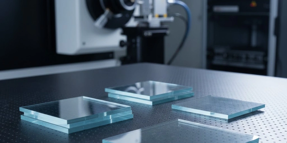
Üretim hattı standartları yerine amaca yönelik gereksinimlere göre üretilen özel alt tabakalar, katalog seçimiyle kesinlikle ulaşılamayan bir parametrik alanın kapılarını açar. Özel üretimde elde edilebilen teknik özellikler, standart ürünlerden sadece derecesi açısından değil, niteliği açısından da farklılık gösterir; bu da sistemin uygulanabilirliğini belirleyen niteliksel yetenek sınırlarını temsil eder.
Katalog Sınırlarının Ötesinde Boyutsal Toleranslar
Hassas özel imalatın tolerans kapasitesi, her geometrik parametre açısından katalog üretimi ile karşılaştırıldığında bir mertebe fark gösterir ve bu fark, yüksek hassasiyetli optik sistemlerde özel spesifikasyonun benimsenmesinin temel teknik gerekçesidir.
Özel erimiş silika imalatında, dış çap toleransları rutin olarak ±0,01 mm ile ±0,025 mm arasında elde edilmektedir., standart katalog plakalarında tipik olarak görülen ±0,1 mm ile ±0,25 mm aralığına kıyasla — hassas oturma gerektiren her türlü mekanik arayüz için belirleyici öneme sahip on katlık bir iyileştirme. Özel üretimde kalınlık toleransları, standart ±0,1 mm ile ±0,2 mm aralığına karşılık ±0,01 mm ile ±0,02 mm aralığına ulaşır; bu da etalon, interferometrik ve dispersif kompanzasyon uygulamaları için gerekli olan hassas optik yol uzunluğu kontrolünü mümkün kılar. Özel imalat levhalarda 10 yay saniyesinin altındaki seviyelerde paralellik sağlanabilir — standart katalog öğeleri için 1–5 yay-dakika olan değere kıyasla — görüntüleme ve koherent algılama sistemlerinde iletilen dalga cephesi eğim hatasını doğrudan azaltan 6 ila 30 katlık bir iyileşme.
Bu toleranslandırma yeteneklerinin pratikteki sonucu, özel üretim kuvars plakaların, bir cihaz montajındaki diğer herhangi bir işlenmiş bileşenle aynı hassasiyette bir mekanik çizime uyacak şekilde tasarlanabilmesidir; bu sayede, standart bir plakanın kalıntı geometrik uyumsuzlukla monte edilmesi durumunda ortaya çıkan şimleme, ayarlama ve tekrarlanan yeniden hizalama döngüleri ortadan kalkar.
Boyutsal Tolerans Karşılaştırması
| Parametre | Standart Katalog Plakaları | Özel İmalat Levhalar |
|---|---|---|
| Dış Çap / Kenar Uzunluğu Toleransı (mm) | ±0,10 ile ±0,25 arası | ±0,01 ile ±0,025 arası |
| Kalınlık Toleransı (mm) | ±0,10 ile ±0,20 arası | ±0,01 ile ±0,02 arası |
| Paralellik (ark saniye) | 60 ila 300 | < 10 |
| Kenar Dikliği (ark dakikası) | 2 ila 5 | < 1 |
| Pah / Eğim Toleransı (mm) | ±0.3 | ±0.05 |
Özel Üretimde Yüzey Şekli ve Yüzey Kalitesi Parametreleri
Özel üretimde yüzey şekli ve yüzey kalitesi özellikleri, katalog üretiminde mevcut olan belirli kalite sınıflarıyla sınırlı değildir ve elde edilebilen özelliklerin tam yelpazesi, standart levhaların sunabileceğinin çok ötesine uzanmaktadır.
Yüzey şekli — cilalı yüzeyin kusursuz bir düzlemden sapması — özel üretimde λ/20 seviyesinde (632,8 nm'de P-V) ölçülebilir ve sertifikalandırılabilir, bu da açık açıklık boyunca 31,6 nm’lik bir fiziksel yüzey sapmasına karşılık gelir. Standart katalog plakaları genellikle λ/4 veya λ/10 olarak sertifikalandırılır; bu değerler sırasıyla 158 nm ve 63,3 nm’lik yüzey sapmalarını temsil eder. Fizeau interferometrisi, koherent ışın birleştirme ve adaptif optik dalga cephesi algılama gibi dalga cephesi açısından kritik uygulamalarda, λ/10 ve λ/20 alt tabaka şekil hatası arasındaki fark, sisteme doğrudan yansır. Strehl oranı2: λ/10 büyüklüğündeki bir iletilen dalga cephesi hatası, eksen üstü Strehl oranını yaklaşık 0,67’ye düşürürken, λ/20 büyüklüğündeki bir hata, kırınım sınırlı bir tasarımda 0,90’ın üzerinde bir Strehl oranı sağlar. Özel üretimde yüzey kalitesi 10⁻⁵ çizik-oyuk seviyesine ulaşır, standart plakalarda bu oran 60-40 iken; bu fark, 1064 nm'deki BRDF ölçüm verilerine göre, yüksek güçlü lazer uygulamalarında yüzey saçılımını standart kalitedeki alt tabakalara kıyasla iki mertebeden fazla azaltmaktadır.
Özel sertifikalı alt tabakalarla birlikte sunulan Fizeau interferometre haritaları, mühendislere şekil hatası dağılımı hakkında uzamsal bilgi sağlar — düşük uzamsal frekanslı şekil hatası (güç, astigmatizm, koma) ile orta uzamsal frekanslı dalgalanma arasında ayrım yaparak, mühendislere şekil hatalarının dağılımı hakkında uzamsal bilgiler sunar; bu da, yalnızca bir teknik özellik numarasıyla elde edilmesi mümkün olmayan sistem düzeyinde dalga cephesi hatası bütçelemeyi mümkün kılar.
Yüzey Özellikleri Karşılaştırması
| Şartname | Standart Katalog | Özel Üretim |
|---|---|---|
| Yüzey P-V Grafiği (632,8 nm'de) | λ/4 ile λ/10 arası | λ/10 ile λ/20 arası |
| Yüzey Kalitesi (Çizik-Çukur) | 60-40'tan 80-50'ye | 10-5'ten 40-20'ye |
| İletilen Dalga Cephesi Hatası (λ) | λ/4 tipik | λ/10 ile λ/20 arası |
| Yüzey Pürüzlülüğü Ra (nm) | 1'den 3'e kadar | < 0.5 |
| İnterferometrik Harita Sertifikasyonu | Mevcut değil | Adet başına satılır |
Özel Uygulamalar için Malzeme Sınıfı Seçimi
Sipariş sırasında malzeme kalitesini belirleme ve uygunluğu teyit eden, partiye özgü malzeme sertifikasını alma imkânı, standart katalog tedarikinde karşılığı bulunmayan, özel imalata özgü bir özelliktir.
800–1200 ppm hidroksil (OH) içeriği ile karakterize edilen JGS1 erimiş silika, 193 nm dalga boyunda 85%’yi aşan iç geçirgenlik sağlar ve derin UV litografi optikleri, eksimer lazer pencereleri ve VUV spektroskopisi alt tabakaları için uygun bir malzemedir. OH içeriği 30 ppm'nin altında olan JGS2, 2,0–2,7 µm aralığında 0,002 cm⁻¹'nin altında emilim gösterir; bu da onu, telekom dalga boylarında çalışan yakın kızılötesi spektroskopi ve fiber bağlantılı algılama uygulamaları için tercih edilen seçenek haline getirir. Doğal kuvars eritme yerine kimyasal buhar biriktirme yöntemiyle üretilen sentetik erimiş silika, 1 ppm'nin altında metalik safsızlık seviyelerine ve 1000 ppm arasında kontrol edilebilen OH içeriğine ulaşır; bu da tek bir malzeme sınıfı içinde hem UV hem de IR performansının hassas bir şekilde belirlenmesini sağlar. Özel imalatta mühendis, sadece malzeme kategorisini değil, aynı zamanda belirli kalite sınıfını, OH içeriği aralığını ve gerekli parti sertifikasını da belirtir — Herhangi bir ciddi optik sistem kalite yönetim sürecinin temelini oluşturan bir düzeyde malzeme izlenebilirliği.
Malzeme Sınıfı Şartnamesi
| Sınıf | OH İçeriği (ppm) | UV Kesimi (nm) | IR Emme Sınırı (µm) | Birincil Uygulama |
|---|---|---|---|---|
| JGS1 | 800–1200 | ~150 | ~2.5 | Derin UV, Eksimer Lazer |
| JGS2 | < 30 | ~165 | ~3.5 | NIR Spektroskopisi, Telekomünikasyon |
| Sentetik (UV) | < 1 | ~150 | ~2.5 | Lazer Sınıfı, Yüksek Güç |
| Sentetik (IR) | > 1000 | ~165 | ~4.0 | Orta Kızılötesi Algılama |
Standart Plakaları Standart Dışı Uygulamalara Zorla Uyarlamanın Gizli Maliyetleri
Standart formatlı bir alt tabakanın, teknik özellik sınırlarını aşan bir uygulamaya monte edilmesi, performans eksikliğini ortadan kaldırmaz — bu eksikliğin maliyetini proje yaşam döngüsünün daha sonraki ve daha pahalı bir aşamasına erteler.
Boyutsal Uyumsuzluk ve Yeniden İşleme Döngüleri. Kalınlığın ±0,05 mm aralığında tutulması gereken bir boşluğa, ±0,2 mm kalınlık toleransına sahip standart bir plaka takıldığında, sistem ya kabul testinden geçemez ya da teknik özelliklerin altında performans gösterir. Her iki durumda da alt tabaka çıkarılmalı ve değiştirilmelidir; bu da yeniden entegrasyon işçiliği, yeniden hizalama süresi ve başarısız entegrasyon sırasında sonraki aşamadaki bileşenlerin gerilime maruz kalması veya kirlenmiş olma olasılığını beraberinde getirir. Belgelenmiş lazer sistemi entegrasyon programlarında, standart plaka boyutlarının uygunsuzluğundan kaynaklanan alt tabaka ile ilgili yeniden işleme döngüleri, etkilenen her bir kavite konumu başına entegrasyon sürelerini 2 ila 6 hafta uzatmıştır., üstelik yeniden işleme işçilik maliyeti, standart levha fiyatı ile özel imalat maliyeti arasındaki farkın genellikle üç ila beş katını aşıyor.
Optik Performans Kayıpları ve Hata Bütçesi Tüketimi. Dalga cephesi açısından kritik bir konuma yerleştirilen standart sınıf bir alt tabaka, yüzey şekil hatasının tamamını sistem dalga cephesi hata bütçesine katar. Sistem, her bir geçirgen eleman için λ/10 dalga cephesi hatası tahsisi ile tasarlanmışsa ve monte edilen plaka — standart katalog ürünlerinde yaygın olduğu gibi — λ/4 değerinde bir hata veriyorsa, λ/6,7'lik fazla hata, diğer elemanlardaki toleransların sıkılaştırılmasıyla telafi edilmeli ya da kalıcı bir performans kaybı olarak kabul edilmelidir. Ölçüm belirsizliğinin dalga cephesi kalitesiyle doğru orantılı olduğu interferometrik cihazlarda, λ/4'lük bir alt tabaka hatası ile λ/10'luk özel üretim bir alt tabaka hatası arasındaki fark, ölçüm gürültü tabanında 2,5 katlık bir artışa yol açar., bu sonuç satın alma kayıtlarında görünmez olsa da sistem performans verilerinde tam olarak ortaya çıkmaktadır.
Vakum Uygulamalarında Sızdırmazlık Arızaları ve Kirlenme Riski. Standart plaka dış çap toleransları olan ±0,25 mm, UHV gözetleme penceresi tertibatlarındaki hassas işlenmiş O-ring oluğu toleransları olan ±0,05 mm ile uyumsuzdur. Bunun sonucunda ortaya çıkan sızdırmazlık uyumsuzluğu, kaba vakum algılama eşiklerinin altında kalma potansiyeli olsa da, 10⁻⁸ Torr'un altında çalışan proses ortamlarına hidrokarbon kirliliği girmesine neden olacak düzeyde sızıntı oranlarına yol açmaktadır. Yarı iletken biriktirme odasında meydana gelen tek bir kontaminasyon olayı, odanın tamamen havalandırılması, fırınlama işlemi ve yeniden onay döngüsünü gerektirir — bu sonucun işletme maliyeti, boyutları kontrol edilmiş özel bir alt tabaka yerine standart bir levha tercih edilmesiyle elde edilen tasarrufların çok ötesindedir.
Kaplama Yeniden Birikim Kayıpları. Bir kaplama sistemine takılan standart bir plaka, ışın izi ile kaplanan bölge arasındaki açıklık hizasızlığı nedeniyle sistem düzeyinde iletim testinden geçemediğinde, plaka, alt tabaka yüzeyinde hasar oluşmadan sıyırma kimyasalına dayanabiliyorsa, sıyırılmalı ve yeniden kaplanmalıdır. Yansıma önleyici kaplamanın sökülmesi ve yeniden uygulanması, her parti için 5 ila 15 iş günü kadar üretim süresi artışı gerektirir ve özellikle yüzey pürüzlülüğü gereksinimleri angstromun altında olan alt tabakalarda, kimyasal sıyırma işleminden kaynaklanan yüzey kalitesinde bozulma riskini beraberinde getirir.
Önemli Dalga Boyu Aralıklarında Özel Kuvars Plakalar için Optik Performans Karşılaştırmaları
Derin UV’den orta kızılötesine kadar tüm spektral aralıkta, erimiş silika alt tabakaların optik performansı, malzeme saflığı, yüzey kalitesi ve üretim hassasiyeti tarafından belirlenir; bu faktörler, her dalga boyu bandında özel üretim plakaları standart katalog ürünlerinden ayıran unsurlardır. Teknik özellik tablosundaki iddialar değil, ölçülen performans verileri, nelerin başarılabileceğini ve bir sistem tasarımcısının pratikte nelere güvenebileceğini belirler.
UV Sınıfı Levhalarda Ultraviyole Geçirgenliği ve Hasar Eşiği
Erişmiş silikanın ultraviyole performansı, onu tüm rakip optik malzemelerden en belirgin şekilde ayıran özelliktir; elde edilebilecek spesifik performans seviyesi ise büyük ölçüde malzeme sınıfına ve yüzey kalitesine bağlıdır — bu iki unsur da yalnızca özel üretimde hassas bir şekilde belirlenebilir.
JGS1 ve sentetik UV sınıfı erimiş silika, 193 nm’de (ArF eksimer lazer dalga boyu) 85–90% iç geçirgenlik sağlar 10 mm kalınlığındaki bir numune için; buna karşılık borosilikat cam, yaklaşık 300 nm’nin altında opak hale gelir. 248 nm'de (KrF eksimer), aynı kalınlıkta geçirgenlik 92%'nin üzerine çıkar ve 266 nm'de (dört katına çıkarılmış Nd:YAG), iç geçirgenlik 95%'yi aşar. 193 nm dalga boyunda UV sınıfı özel üretim kuvars plakaların lazer kaynaklı hasar eşiği (LIDT), 15–25 mJ/cm² (10 ns darbe süresi) olarak ölçülmüştür. ISO 21254 standardına uygun bire bir test protokolleri kullanılarak; burada yüzey kalitesi en belirleyici faktördür — 10-5 çizik-oyuk yüzeyler, hasar bölgesinde fototermal ortak yol interferometrisi ile ölçüldüğünde, eşdeğer fluans koşullarında 60-40 yüzeylere kıyasla tutarlı bir şekilde 40–60% daha yüksek LIDT değerleri sergilemektedir.
UV sınıfı erimiş silikanın solarizasyon direnci — yani uzun süreli UV maruziyeti altında geçirgenliğini koruma yeteneği — aynı zamanda OH içeriğinin bir fonksiyonudur; yüksek OH içeriğine sahip JGS1 malzemesi, nokta kusur bölgelerinde renk merkezi oluşumunu bastırmada Si-OH bağlarının oynadığı rol sayesinde üstün solarizasyon direnci sergilemektedir.
UV Geçişi ve LIDT Verileri
| Malzeme Sınıfı | 193 nm'de geçirgenlik (%) | 248 nm'de geçirgenlik (%) | 193 nm'de LIDT, 10 ns (mJ/cm²) | Yüzey Kalitesi |
|---|---|---|---|---|
| JGS1 (10 mm kalınlık) | 85-90 | 92–95 | 15–25 | 10-5 Özel |
| JGS1 (10 mm kalınlık) | 80-85 | 88–92 | 9–14 | 60-40 Standart |
| Sentetik UV sınıfı | 87–92 | 93–96 | 18–28 | 10-5 Özel |
| BK7 (referans) | < 5 | 45–55 | Geçerli değil | 60-40 |
Görünür ve Yakın Kızılötesi Işık Geçirgenliğinin Kararlılığı
Görünür ve yakın kızılötesi dalga boyu aralığında, erimiş silikanın geçirgenlik performansı, olağanüstü bir homojenlik ve kararlılık ile karakterize edilir; bu özellikleri sayesinde BK7 camının üzerinde yer alır ve ilgili dalga boyu aralığının büyük bir kısmında safir ile rekabet edebilir düzeydeyken, aynı zamanda alt tabaka geometrisinde esneklik açısından önemli pratik avantajlar sunar.
Eriyik silika, 400–2000 nm aralığında 92%’nin üzerinde iç geçirgenliği korur 10 mm kalınlığındaki bir numune için, hassas sınıf özel imalatla 100 mm'lik bir açıklık boyunca Δn < 5 × 10⁻⁶ düzeyinde kırılma indisi homojenliği elde edilebilir — buna karşılık, standart katalog malzemelerinde tipik olarak Δn < 5 × 10⁻⁵ değerine ulaşılır. Kırılma indisi homojenliğindeki bu mertebe düzeyindeki iyileşme, iletilen dalga cephesi kalitesine doğrudan yansır: 3 mm kalınlığındaki bir plaka üzerinde 5 × 10⁻⁶ kırılma indisi homojenliği, 633 nm'de λ/100'den daha az bir dalga cephesi hatasına yol açarken, standart sınıf malzeme homojenliğine sahip aynı kalınlıktaki bir plaka için bu değer λ/10'dur. Telekom dalga boylarında (1310 nm, 1550 nm) gerçekleştirilen interferometrik uygulamalarda, Δn < 5 × 10⁻⁶ değerine sahip özel siparişle üretilmiş erimiş silikanın iletilen dalga cephesi hatası, tutarlı bir şekilde λ/50’nin altındadır. Yayınlanmış bileşen yeterlilik verilerinde bildirilen Zygo GPI interferometre ölçümlerine göre, 80 mm’lik net açıklıklar boyunca.
1064 nm'de karşılaştırmalı geçirgenlik ölçümleri — Nd:YAG temel dalga boyu — özel üretim kuvars plakaların yüzey başına geçirgenliğinin (kaplama öncesi) 99,2–99,51 TP3T olduğu, standart katalog ürünlerinde ise 98,8–99,11 TP3T olduğu görülmüştür; bu fark, standart üretimde daha az agresif parlatma döngülerinden kaynaklanan yüzey altı kalıntı hasarlarına atfedilebilir.
Görünür Işık ve NIR Geçiş Kabiliyeti Karşılaştırması
| Dalga boyu (nm) | Özel Üretim Erimiş Silika (%) | Erimiş Silika Standardı (%) | BK7 Cam (%) | Safir (%) |
|---|---|---|---|---|
| 400 | 93.5 | 91.8 | 91.2 | 85.0 |
| 633 | 93.8 | 92.5 | 92.0 | 86.5 |
| 1064 | 93.9 | 92.9 | 91.5 | 87.2 |
| 1550 | 93.7 | 92.6 | 88.3 | 87.8 |
| 2000 | 91.2 | 89.5 | 72.0 | 86.0 |
Çalışma Koşulları Altında Termal Kararlılık ve Kırılma İndeksi Tekdüzeliği
Çalışma koşulları altında erimiş silikanın termal davranışı, onu yüksek güçlü lazer sistemlerinde, uzayda kullanılan cihazlarda ve termal döngüye maruz kalan hassas ölçüm ekipmanlarında vazgeçilmez kılan özelliktir; bu koşullarda özel olarak üretilmiş plakaların performans avantajı, termal gerilim altında korunan daha sıkı başlangıç yüzey şekli sayesinde daha da artmaktadır.
Erimiş silikanın termal genleşme katsayısı (CTE) 0,55 × 10⁻⁶ /K'dir; buna karşılık BK7 için bu değer 7,1 × 10⁻⁶ /K, safir için ise 5,3 × 10⁻⁶ /K’dir — bu, BK7’ye kıyasla 13 katlık bir avantajdır ve ısı yükü altında termal kaynaklı yüzey şekil değişimini doğrudan belirler. Çapı boyunca 50°C’lik bir sıcaklık gradyanına maruz kalan, 100 mm çapında ve 5 mm kalınlığında özel bir kuvars plaka için, termal kaynaklı güç değişimi yaklaşık 0,028 λ’dir (633 nm’de) — bu, dalga cephesi hata bütçesine ihmal edilebilir düzeyde bir katkıdır. Aynı gradyan altında eşdeğer bir BK7 levha, 0,36 λ'lik termal kaynaklı güç katkısı sağlayacaktır; bu, bir kırınım sınırlı sistemi 0,67'lik bir Strehl oranına düşürmeye yeterlidir. 589 nm dalga boyunda erimiş silikanın termo-optik katsayısı dn/dT, 1,28 × 10⁻⁵ /K'dir, ve 3 mm kalınlığındaki bir alt tabaka için, 10 °C’lik bir sıcaklık değişimi, 3,84 × 10⁻⁴ mm’lik bir optik yol değişikliğine yol açar — bu da 633 nm’de 0,61 λ’ye eşdeğerdir.
−40 °C ile +80 °C arasında termal döngüye maruz kalan uzayda kullanılan cihazlarda, özel üretim erimiş silika alt tabakaların alternatif malzemelere göre sahip olduğu CTE avantajı, alt tabaka-montaj arayüzünde döngüsel gerilimin birikmesini önler; bu gerilim birikimi, tekrarlanan termal dalgalanmaların ardından yüzey şeklinin giderek bozulmasına yol açar — bu arıza türü, 50'den az termal döngüden sonra BK7 tabanlı pencere tertibatlarında belgelenmiştir.
Termal Özelliklerin Karşılaştırılması
| Mülkiyet | Erimiş Silika | BK7 Cam | Safir | Borosilikat |
|---|---|---|---|---|
| CTE (×10⁻⁶ /K) | 0.55 | 7.10 | 5.30 | 3.25 |
| 589 nm'de dn/dT (×10⁻⁵ /K) | 1.28 | 2.40 | 1.32 | 1.10 |
| Maksimum Sürekli Çalışma Sıcaklığı (°C) | 1000 | 500 | 1600 | 460 |
| Termal Şok Direnci | Mükemmel | Orta düzeyde | İyi | İyi |
| Döngüsel Gerilme Arızası (döngü sayısı) | > 1000 | < 50 | > 500 | > 200 |

TOQUARTZ Özel Kuvars Plakaları Neden Zorlu Uygulama Gereksinimlerini Karşılıyor?
Boyutsal toleranslar, uygulamaya özgü gereksinimler ve dalga boyuna göre ayrıştırılmış optik performans açısından özel imalat için parametrik temeli ortaya koyduktan sonra, ortaya çıkan pratik soru, hangi imalat kaynağının hassas optik sistem geliştirmenin gerektirdiği tutarlılık ve belgeleme kalitesiyle bu teknik özellikleri karşılayabileceğidir. TOQUARTZ, tanımlanmış bir malzeme sınıfı portföyü, doğrulanmış tolerans yetenekleri ve bu makalede analiz edilen gereksinimlerin tamamını kapsayan desteklenen geometri aralığı sayesinde bu soruyu ele almaktadır.
TOQUARTZ Aracılığıyla Sunulan Malzeme Sınıfları ve Saflık Standartları
TOQUARTZ, dört ana malzeme sınıfında özel üretim kuvars plakalar sunmaktadır; her bir sınıf, iletim bandı, lazer uyumluluğu ve malzeme saflık seviyesi ile tanımlanan belirli bir performans aralığına yöneliktir.
UV sınıfı JGS1 ürünü, 800–1200 ppm aralığında OH içeriği sunar ve 193 nm dalga boyunda 85%’nin üzerinde sertifikalı iç geçirgenliğe sahiptir, bu da onu eksimer lazer optiği, derin UV litografi ve VUV spektroskopisi uygulamaları için uygun hale getirir. NIR için optimize edilmiş JGS2 sınıfı, OH içeriğini 30 ppm'nin altında tutarak 2,73 µm'lik OH absorpsiyon bandını bastırır ve kullanılabilir geçirgenliği yaklaşık 3,5 µm'ye kadar genişletir — bu, atmosferik eser gaz algılama ve optik koherens tomografi3 genişletilmiş dalga boylarında. Sentetik erimiş silika türleri, hem UV için optimize edilmiş (OH 1000 ppm) konfigürasyonlarda mevcuttur; her parti için ICP-MS analizi ile toplam metalik kirlilik içeriğinin 1 ppm’nin altında olduğu teyit edilmiştir. Her özel siparişle birlikte, partiye özgü malzeme sertifikası verilmektedir, 589 nm'de kırılma indisi ölçümü, FTIR ile OH içeriği doğrulaması ve malzemenin belirtilen dalga boyu aralığı boyunca geçirgenlik ölçümü dahil — bu belgeler, standart katalog kanalları aracılığıyla temin edilememektedir.
TOQUARTZ Malzeme Sınıfı Portföyü
| Sınıf | OH İçeriği (ppm) | UV Kesimi (nm) | NIR Kenar (µm) | Verilen Sertifika |
|---|---|---|---|---|
| JGS1 UV Sınıfı | 800–1200 | ~150 | ~2.5 | FTIR ile OH iletim eğrisi |
| JGS2 NIR Sınıfı | < 30 | ~165 | ~3.5 | FTIR ile OH iletim eğrisi |
| Sentetik UV | < 1 | ~150 | ~2.5 | ICP-MS, FTIR, kırılma indisi |
| Sentetik IR | > 1000 | ~165 | ~4.0 | ICP-MS, FTIR, geçirgenlik |
Özel Siparişler İçin Boyutsal ve Optik Tolerans Olanakları
TOQUARTZ özel kuvars plakaları aracılığıyla sunulan tolerans özellikleri, bu analizde belirlenen tüm hassasiyet gereksinimlerini kapsamaktadır — standart hassasiyetli yedek parçalardan, her biri ayrı Fizeau sertifikasına sahip interferometre sınıfı alt tabakalara kadar.
Kalınlık toleransları ±0,10 mm’den (üretim sınıfı) ±0,01 mm’ye (hassas sınıf) kadar mevcuttur, standart yedek parça uygulamalarından etalon ve rezonans boşluğu bileşenlerine kadar tüm yelpazeyi kapsamaktadır. Dış çap ve kenar uzunluğu toleransları, hassas sınıf üretimde ±0,01 mm’ye ulaşarak UHV gözetleme penceresi flanşları ve kinematik lens yuvalarının geçme gereksinimlerini karşılamaktadır. Paralellik, 10 yay saniyesinden daha iyi bir hassasiyette sağlanabilmekte ve Yüzey şekli, 632,8 nm dalga boyunda λ/20 P-V değerine uygunluğu onaylanmıştır; her parça için ayrı Fizeau interferometre haritaları sunulmaktadır. — düşük mertebeden şekil hatalarını orta uzamsal frekans katkılarıyla ayıran uzamsal dağılım verileri de dahil olmak üzere. 10⁻⁵ çizik-çukur seviyesindeki yüzey kalitesi, lazer sınıfı ve interferometrik sınıf spesifikasyonları için mevcuttur; sapma ışığına duyarlı uygulamalar için ise talep üzerine BRDF ölçüm verileri sağlanabilir.
TOQUARTZ Özel Tolerans Yetenekleri
| Parametre | Üretim Sınıfı | Hassas Sınıf | İnterferometre Sınıfı |
|---|---|---|---|
| Kalınlık Toleransı (mm) | ±0.10 | ±0.05 | ±0.01 |
| Çap / Kenar Toleransı (mm) | ±0.05 | ±0,025 | ±0.01 |
| Paralellik (ark saniye) | < 60 | < 30 | < 10 |
| Yüzey Şekli P-V (λ = 632,8 nm) | λ/4 | λ/10 | λ/20 |
| Yüzey Kalitesi (Çizik-Çukur) | 60-40 | 40-20 | 10-5 |
| Bireysel İnterferometre Haritası | Hayır | Opsiyonel | Standart |
Özel Üretim İçin Desteklenen Geometriler ve Form Faktörleri
TOQUARTZ’ın özel imalat yetenekleri, bu analizde belgelenen tüm açıklık geometrilerini kapsamaktadır — standart dairesel ve dikdörtgen formatlardan, hassas profilli dairesel olmayan alt tabakalara ve pahlar, eğimli kenarlar ve deliklere sahip çok özellikli plakalara kadar.
Çapı 5 mm ile 300 mm arasında değişen dairesel plakalar mevcuttur, fiber bağlantılı mikro-optiklerden geniş açıklıklı teleskop ikincil camlarına kadar tüm yelpazeyi kapsamaktadır. Dikdörtgen ve kare formatlar 5 mm × 5 mm’den 200 mm × 200 mm’ye kadar uzanır; yarık geometrili spektroskopik uygulamalar için 10:1’e kadar en-boy oranları mevcuttur. Eliptik, çokgen ve özel CAD tanımlı konturlar dahil olmak üzere dairesel olmayan profiller, CNC su jeti profilleme yöntemiyle üretilir ve ardından ısıdan etkilenen bölgeyi ortadan kaldırmak ve kenar dikliğini 1 ark dakikası hassasiyetinde geri kazanmak için kenar parlatma işlemi uygulanır. İsteğe bağlı imalat hizmetleri arasında hassas pah kırma (0,1 mm ila 2 mm, ±0,05 mm tolerans), minimum 0,5 mm çapa kadar lazerle delinmiş geçiş delikleri ve temiz oda Sınıf 10 standardına uygun AR veya HR kaplama öncesi temizlik yer almaktadır. — ek yüzey hazırlık aşamalarına gerek kalmaksızın, kaplama uygulamasına hemen hazır alt tabakaların alınmasını sağlar.
Desteklenen Geometri ve Form Faktörü Aralığı
| Özellik | Şartname |
|---|---|
| Dairesel Çap Aralığı (mm) | 5 ila 300 |
| Dikdörtgen Maksimum Boyut (mm) | 200 × 200 |
| Minimum En-Boy Oranı | 1:1 |
| Maksimum En-Boy Oranı | 10:1 |
| Dairesel Olmayan Profiller | Eliptik, çokgen, özel CAD |
| Pah Toleransı (mm) | ±0.05 |
| Delikten Geçen Parçanın Minimum Çapı (mm) | 0.5 |
| Kenar Dikliği (ark-dakika) | < 1 |
Sisteminiz İçin Özel Bir Kuvars Plaka Belirlemeden Önce Kontrol Listesi
Üretim aşamasına girerken çözülmemiş bir belirsizlik içeren her özel alt tabaka spesifikasyonu, denetim aşamasında bir uygunsuzluğa yol açar. Aşağıdaki kontrol listesi, bu makale boyunca geliştirilen tüm parametrik çerçeveyi, üretime hazır bir özel kuvars plaka spesifikasyonunun yayınlanabilmesi için önceden tanımlanması gereken asgari değişkenler kümesine özetlemektedir.
-
Dalga Boyu Aralığı ve Malzeme Sınıfı — Uygulama dalga boyunun derin UV ( 2 µm, JGS2 veya sentetik kızılötesi gerektirir) aralığına mı, yoksa her iki sınıfın da uygun olduğu görünür/standart kızılötesi aralığına mı girdiğini teyit edin. Uygulama 2,73 µm emilim bandına duyarlıysa OH içeriği aralığını belirtin.
-
Dış Geometri ve Boyutsal Toleranslar — Açıklığın şeklini (dairesel, dikdörtgen, eliptik, özel), tüm doğrusal boyutları ve mekanik arayüz için gerekli boyut toleranslarını tanımlayın. İşlevsel açık açıklık ile toplam alt tabaka dış hatları arasında ayrım yapın ve konum ve boyut toleranslarıyla birlikte tüm pahları, eğimleri veya geçiş deliklerini belirtin.
-
Kalınlık ve Paralellik — Nominal kalınlığı, izin verilen kalınlık toleransını (etalon veya kavite uygulamaları için ±0,01 mm, genel geçirgenlik için ±0,05 mm) ve yay saniyesiyle ifade edilen gerekli paralellik değerini belirtiniz. Koherent uygulamalar için, kaynağın koherans uzunluğu bağlamında izin verilen maksimum kama açısını da belirtiniz.
-
Yüzey Şekli ve Geçen Dalga Cephesi Hatası — Test dalga boyunda (tipik olarak 632,8 nm) yüzey şekli P-V değerini λ birimlerinde belirtin ve bu spesifikasyonun yansıyan dalga cephesi (yüzey şekli) mi yoksa geçirilen dalga cephesi (kütle homojenliği dahil) mi için geçerli olduğunu teyit edin. İnterferometrik uygulamalar için, uzamsal frekans ayrıştırmasına sahip ayrı Fizeau haritaları talep edin.
-
Yüzey Kalitesi — MIL-PRF-13830B standardına göre gerekli çizilme-kazıma spesifikasyonunu belirtiniz. Yüksek güçlü lazer uygulamaları için, giriş yüzünde 10-5 değerini belirtiniz ve çıkış yüzünde aynı işlemin mi yoksa daha esnek bir spesifikasyonun mu gerekli olduğunu teyit ediniz.
-
Lazer Hasar Eşiği — Başvuru, darbeli veya sürekli dalgalı (CW) lazer ışınlamasını içeriyorsa, minimum LIDT değerini mJ/cm² veya W/cm² cinsinden belirtin, darbe süresini, dalga boyunu ve tekrarlama hızını belirtin ve imalatçıdan, yüzey kalitesi derecesinin ve kaplamanın (varsa) ISO 21254 test koşulları altında belirtilen LIDT gerekliliğini karşılayıp karşılamadığını teyit etmesini isteyin.
-
Sertifikasyon ve Belgeler — Gerekli belge paketini belirtin: partiye özgü malzeme sertifikası, ayrı interferometrik yüzey şekil haritası, geçirgenlik eğrisi, OH içeriği ölçümü, temizlik seviyesi ve uygulamaya özgü tüm yeterlilikler (UHV uyumluluğu, ECSS uzay yeterliliği, MIL-spec uyumluluğu).
Sonuç
Bu analizde derlenen teknik veriler son derece nettir: Standart katalogda yer alan erimiş silika plakaların performans sınırları, optik sistem gereksinimleri tarafından değil, üretim ekonomisi tarafından belirlenmektedir. Boyutsal tolerans, açıklık geometrisi, yüzey kalitesi veya dalga boyuna özgü performans gibi uygulama kısıtlamaları bu sınırları aştığında — ki bu durum yarı iletken işleme, lazer sistemi entegrasyonu, hassas spektroskopi ve havacılık ve uzay enstrümantasyonunda sıklıkla görülür — özel üretim kuvars plakalar lüks bir seçenek değil, teknik bir zorunluluktur. Özel imalat yoluyla elde edilebilen geometri, yüzey kalitesi, malzeme sınıfı ve sertifikasyon özellikleri, kademeli bir iyileştirmeden ziyade niteliksel bir kapasite artışı anlamına gelir. Yukarıda sunulan kontrol listesi çerçevesini takip ederek, imalatçıyla çalışmaya başlamadan önce tüm parametre setini tanımlamak, sistem tasarımından uyumlu alt tabaka teslimatına kadar uzanan en güvenilir yoldur.
SSS
Özel üretim kuvars plakalar sadece büyük miktarlı üretim siparişleri için mi uygun olur?
Özel kuvars plakalar, miktardan bağımsız olarak hassas boyutsal ve optik özelliklere göre üretilmektedir; ayrıca, CNC parlatma ve profilleme iş akışlarının daha esnek hale gelmesiyle birlikte, hassas üretim yapan firmalarda özel alt tabakalar için minimum sipariş miktarları önemli ölçüde azalmıştır. Tek parça ve bir ila on adetlik küçük parti siparişler, uzmanlaşmış erimiş silika imalatçıları tarafından rutin olarak karşılanmaktadır; bu da özel spesifikasyonları, yalnızca yüksek hacimli üretim için değil, prototip, araştırma ve düşük hacimli cihaz üretimi bağlamlarında da ekonomik olarak uygulanabilir hale getirmektedir.
Optik uygulamalarda erimiş silika ile kuvars camı arasındaki fark nedir?
Eriyik silika ve kuvars camı, her ikisi de amorf silikon dioksit (SiO₂) olmakla birlikte, üretim yöntemleri ve elde edilen saflık düzeyleri bakımından farklılık gösterir. Doğal kuvars, kristal kuvars mineralinden eritilerek elde edilir; bu işlem sonucunda ppm düzeyinde eser miktarda metalik safsızlıklar ve değişken OH içeriğine sahip bir malzeme ortaya çıkar. Sentetik erimiş silika, silikon tetraklorür veya silanın kimyasal buhar biriktirme yöntemiyle üretilir; bu yöntem, 1 ppm'nin altında metalik safsızlık seviyeleri ve hassas bir şekilde kontrol edilebilen OH içeriği sağlar. Derin UV veya yüksek lazer güç yoğunluklarındaki optik uygulamalar için sentetik erimiş silika tercih edilirken, saflık farkının spesifikasyon dahilindeki performansı etkilemediği görünür ışık ve NIR uygulamaları için doğal eritme malzemesi (JGS1, JGS2) uygundur.
Bir alt tabakanın yüzey şekli özellikleri, sistem dalga cephesi hatasını nasıl etkiler?
Düzlem-paralel erimiş silika plakanın iletilen dalga cephesi hatası (TWE), hem giriş hem de çıkış yüzlerindeki yüzey şekli hem de hacim kırılma indisi düzensizliğinden kaynaklanan etkileri içerir. Her yüzünde λ/10 yüzey şekline ve 3 mm kalınlık boyunca Δn = 5 × 10⁻⁶ kırılma indisi homojenliğine sahip bir plaka için, toplam TWE'de yüzey şekli baskındır ve çift geçişte 633 nm'de yaklaşık λ/5'lik bir katkı sağlar. Yüzey başına λ/20 ve Δn < 5 × 10⁻⁶ değerlerinde sertifikalandırılmış özel üretim alt tabakalar, toplam TWE katkısını λ/10'un altına indirerek diğer sistem elemanları için dalga cephesi bütçesini korur.
Özel üretim kuvars plakalar, yansıma önleyici kaplamalar önceden uygulanmış olarak temin edilebilir mi?
Evet — özel üretim erimiş silika alt tabakalar, son parlatma ve boyutsal kontrol işlemlerinden sonra üzerine yansıma önleyici, kısmi yansıma veya bant geçiren kaplamalar uygulanmış olarak teslim edilebilir. Kaplama özellikleri, alt tabaka yüzey kalitesiyle uyumlu olmalıdır; çünkü iyon ışını püskürtme ve elektron ışını buharlaştırma gibi kaplama işlemleri, yüzey pürüzlülüğüne ve temizliğine bağlı olarak yapışma ve gerilme gereksinimleri getirir. Son kullanıcı tarafından teslimattan sonra kaplanacak alt tabakalar, temiz oda Sınıf 10 standartlarına uygun bir ön temizlik aşaması ile belirtilmeli ve nakliye ve depolama sırasında yüzey temizliğini korumak için azotla temizlenmiş, çift sızdırmaz kaplarda paketlenmelidir.
Referanslar:
-
Bu makale, Fabry-Pérot interferometrelerinin çalışma prensibini açıklamakta olup, alt tabaka kalınlığı ve paralellik hatalarının serbest spektral aralığı ve inceliği nasıl etkilediğini de ele almaktadır.↩
-
Bu makale, Strehl oranını optik sistem kalitesinin bir ölçüsü olarak tanımlamakta; dalga cephesi hatasıyla olan matematiksel ilişkisini ve kırınım sınırlı sistemlerin değerlendirilmesindeki kullanımını açıklamaktadır.↩
-
Bu metin, OCT görüntüleme sistemlerinin çalışma prensiplerini ve sistem performansını belirleyen — alt tabaka geçirgenliği ve dağılımı da dahil olmak üzere — optik bileşen gereksinimlerini açıklamaktadır.↩