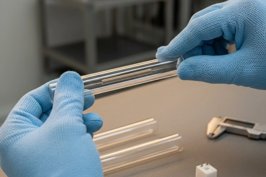
Допуски толщины кварцевых пластин оптического качества играют важную роль в определении качества и надежности современных оптических систем. Для большинства приложений требуются допуски от ±0,01 мм до ±0,1 мм, в зависимости от требований к производительности. В таблице ниже приведены общие уровни допусков для прецизионной оптики:
Уровень толерантности | Допуск на толщину по центру (мм) |
|---|---|
Уровень 4 | ±0.005 |
Уровень 11 | ±0.010 |
Уровень 2 | ±0.1 |
Уровень 5 | ±0.25 |
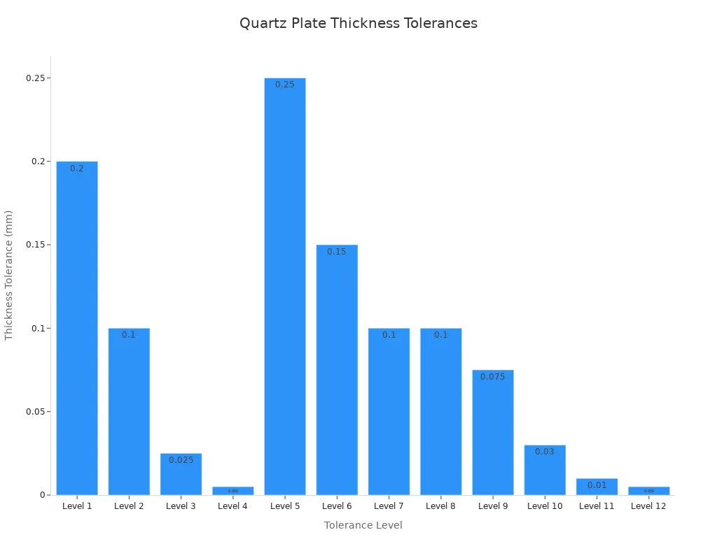
Более жесткие допуски улучшают оптические характеристики, но при этом увеличивают стоимость производства. Классы прецизионных, высокоточных и базовых допусков влияют как на точность системы, так и на ее стоимость.
Основные выводы
Для обеспечения высокой производительности в оптических системах кварцевые пластины оптического класса должны иметь определенные допуски по толщине. Обычные допуски составляют от ±0,01 мм до ±0,1 мм.
Более жесткие допуски улучшают оптические характеристики, но могут увеличить стоимость производства. Баланс - это ключ к достижению качества и доступности.
Такие области применения, как прецизионная интерферометрия и лазерная оптика, требуют строгого контроля толщины для минимизации ошибок волнового фронта и обеспечения высокого качества результатов.
При производстве полупроводников допуски по толщине ±0,03-0,05 мм имеют решающее значение для поддержания равномерности температуры и максимизации выхода продукции.
Выбор правильного допуска в зависимости от потребностей приложения помогает инженерам избежать лишних затрат и обеспечить оптимальную производительность.
Какие допуски по толщине требуются для прецизионной интерферометрии и лазерной оптики?

Прецизионная интерферометрия и лазерная оптика требуют строгого контроля над кварцевая пластина оптического качества допуски по толщине. Эти допуски непосредственно влияют на погрешность волнового фронта, качество передачи и плоскостность, что крайне важно для высокопроизводительных оптических систем. Отраслевые стандарты, такие как ISO 10110, MIL и ASTM, определяют выбор соответствующих допусков для каждого применения.
Стандартные окна интерферометра: характеристики допуска ±0,25 мм (±0,010")
Стандартные окна интерферометров обычно имеют допуск по толщине ±0,25 мм (±0,010"). Такой уровень допуска гарантирует, что разница оптических путей остается в приемлемых пределах для большинства задач интерферометрии видимой длины волны. Сочетание допуска по толщине, параллельности и плоскостности определяет общую точность измерений.
Окно с допуском ±0,25 мм может поддерживать ошибку волнового фронта в пределах λ/4 при длине волны 632,8 нм, что подходит для общей метрологии и оптических испытаний. В следующей таблице приведены данные о влиянии допуска по толщине на основные оптические параметры:
Аспект | Эффект |
|---|---|
Ошибка волнового фронта | Искривление из-за напряжения покрытия увеличивает погрешность, вызывая смещение фокуса и искажение пятна. |
Трансмиссия | Неровности толщины влияют на ошибку передаваемого волнового фронта (TWE). |
Плоскость | Более толстые подложки противостоят искривлению, улучшая плоскостность. |
Этот уровень допуска позволяет сбалансировать стоимость и производительность, что делает его распространенным выбором для стандартных интерферометрических приложений.
Точность лазерных систем: ±0,13 мм (±0,005") с контролем TTV
В прецизионных лазерных системах часто задается более жесткий допуск по толщине ±0,13 мм (±0,005 дюйма) и требуется строгий контроль общей вариации толщины (TTV). Эти требования помогают минимизировать искажения волнового фронта и тепловое линзирование, которые могут ухудшить качество лазерного луча. Высокомощные и импульсные лазерные системы выигрывают от такой точности, поскольку даже небольшие отклонения толщины могут вызвать значительные различия в оптическом пути.
Производители добиваются таких допусков благодаря передовым методам шлифовки и полировки, а также строгим протоколам контроля. Ниже перечислены основные причины таких спецификаций:
Минимизирует ошибку волнового фронта и тепловое линзирование
Повышает порог лазерно-индуцированного повреждения
Обеспечивает постоянное качество луча по всей апертуре
Соблюдая эти допуски на толщину кварцевых пластин оптического класса, инженеры могут оптимизировать производительность и надежность системы в сложных лазерных приложениях.
Эталонные оптические плоскости: сверхточный допуск ±0,05 мм (±0,002 дюйма)
Эталонные оптические плоскости требуют самых строгих допусков по толщине, часто достигающих ±0,05 мм (±0,002 дюйма). Эти сверхточные компоненты служат калибровочными стандартами для других оптических элементов. Жесткий допуск обеспечивает минимальное расхождение оптического пути и поддерживает высочайший уровень точности измерений.
В таблице ниже приведены типичные допуски для оптических элементов:
Параметр | |
|---|---|
Толщина | 0,2 мм (исходный уровень) |
0,05 мм (точность) | |
0,01 мм (высокая точность) |
Сверхточные допуски на толщину кварцевых пластин оптического класса необходимы для приложений, где даже самое незначительное отклонение может повлиять на калибровку и прослеживаемость.
Оптика для ультрафиолетового и глубокого ультрафиолета: более жесткие допуски для более коротких длин волн
Оптика для ультрафиолетового и глубокого ультрафиолета требует еще более жестких допусков по толщине из-за более коротких длин волн. При уменьшении длины волны одно и то же изменение толщины приводит к увеличению разницы оптического пути, что делает точность еще более критичной. Типичные допуски для высокоточной УФ-оптики могут достигать 10 мкм.
Приведенная ниже диаграмма иллюстрирует соотношение между базовыми, прецизионными и высокоточными допусками для УФ-оптики:
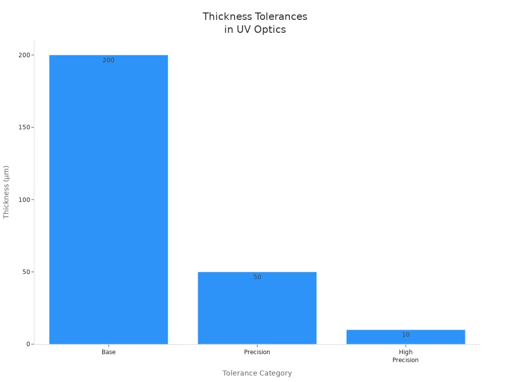
Короткие длины волн усиливают влияние ошибок толщины
Для высокоточной УФ-оптики часто требуются допуски 10-50 мкм.
Однородность материала и качество поверхности также становятся более важными
Выбор правильных допусков на толщину кварцевой пластины оптического качества для применения в ультрафиолетовых и глубоких ультрафиолетовых лучах обеспечивает оптимальную производительность и точность измерений.
Какие допуски по толщине требуются для компонентов оборудования для производства полупроводников?

Оборудование для производства полупроводников полагается на точные допуски толщины кварцевых пластин для обеспечения стабильности процесса и выхода продукции. К каждому компоненту, от держателей пластин до смотровых окон, предъявляются уникальные требования, основанные на его назначении и необходимом уровне контроля процесса. Понимание этих различий помогает инженерам выбрать правильную спецификацию, обеспечивающую как производительность, так и экономическую эффективность.
Обработка 300-миллиметровых пластин: ±0,03-0,05 мм для критической тепловой однородности
Инженеры указывают жесткие допуски по толщине ±0,03-0,05 мм для компонентов обработки 300-миллиметровых пластин. Такой уровень контроля необходим, поскольку даже небольшие отклонения по толщине могут вызвать значительные температурные градиенты при быстрой термической обработке.
Разница в толщине 0,1 мм на 300-миллиметровой кварцевой пластине может создать разницу в тепловой массе около 30 граммов, что приводит к разнице температур в 4-6°C во время циклов нагрева. Такие перепады могут снизить выход устройств на 3-8%, особенно в передовых полупроводниковых узлах ниже 10 нм. Для решения этой проблемы производители используют кварц высокой чистоты и передовые технологии шлифовки, чтобы добиться общего отклонения по толщине (TTV) менее 0,020 мм, что обеспечивает равномерное распределение тепла и стабильную обработку пластин.
В сводной таблице представлены основные взаимосвязи:
Технические характеристики | Типичное значение | Причинное воздействие |
|---|---|---|
Допуск по толщине | ±0,03-0,05 мм | Регулирует тепловую массу, влияет на равномерность |
TTV | <0,020 мм | Уменьшает температурные градиенты |
Влияние на урожайность | 3-8% потери при выходе | Прямой результат плохого контроля толщины |
Обработка 200-миллиметровых пластин: ±0,08-0,10 мм для стандартных процессов
Для обработки 200-миллиметровых пластин в промышленности допускаются допуски по толщине ±0,08-0,10 мм. Эти компоненты работают при более низких скоростях нагрева и имеют меньшую площадь поверхности, поэтому риск неравномерности температуры снижается по сравнению с 300-мм системами.
Изменение толщины на 0,1 мм в 200-миллиметровой подложке приводит к разнице в тепловой массе около 8-10 граммов, что обычно вызывает температурный градиент в 2-3°C. Такой уровень отклонений остается в пределах допустимого диапазона для большинства стандартных полупроводниковых процессов, где выход устройств менее чувствителен к незначительным температурным колебаниям. Производители часто балансируют между стоимостью и производительностью, выбирая этот допуск, который позволяет эффективно производить продукцию без ущерба для надежности процесса.
Ключевые моменты для обработки 200-миллиметровых пластин:
Допуск ±0,08-0,10 мм поддерживает стандартный контроль процесса
Более низкий риск температурных перепадов по сравнению с 300-миллиметровыми системами
Экономическая эффективность для зрелых полупроводниковых узлов
Поддерживает производительность устройств в соответствии с отраслевыми стандартами
Эти факторы делают ±0,08-0,10 мм практичным выбором для большинства применений 200-миллиметровых пластин.
Газораспределительные и душевые пластины: ±0,08 мм с контролем плоскостности
Для газораспределительных и душевых пластин требуется допуск по толщине ±0,08 мм в сочетании со строгим контролем плоскостности. Эти пластины играют важнейшую роль в обеспечении равномерного потока газа и плотности плазмы в таких процессах, как травление и осаждение.
Отклонение толщины более чем на ±0,10 мм может привести к неравномерности скорости травления, превышающей 3% по всей пластине, что напрямую влияет на контроль критических размеров (CD) и общий выход микросхем. Спецификации плоскостности, такие как ≤0,005 дюйма на фут, помогают поддерживать постоянный зазор между пластиной и подложкой, что очень важно для воспроизводимости процесса. Производители добиваются этих допусков путем прецизионной шлифовки и тщательного контроля, часто с использованием автоматизированных измерительных систем.
Параметр | Типичное значение | Влияние на процесс |
|---|---|---|
Допуск по толщине | ±0,08 мм | Поддерживает равномерность потока газа |
Плоскость | ≤0.005"/ft | Обеспечивает равномерное распределение плазмы |
Равномерность скорости травления | <±3% вариация | Непосредственно связана с толщиной/плоскостью |
Такое сочетание контроля толщины и плоскостности обеспечивает надежность и повторяемость обработки полупроводников.
Смотровые окна печи: ±0,15 мм для некритичного оптического обзора
Для смотровых окон печей используется более мягкий допуск по толщине - ±0,15 мм. Эти компоненты не оказывают прямого влияния на температуру процесса или производительность устройства, поэтому инженеры отдают предпочтение механической прочности и устойчивости к тепловым ударам, а не точности размеров.
Толщина типичного смотрового окна может варьироваться от 3 мм до 20 мм, при этом основным требованием является способность выдерживать многократные термоциклы при температурах до 1200°C. Более широкий допуск снижает стоимость изготовления до 40% по сравнению с прецизионными шлифованными компонентами, что делает его экономически эффективным решением для некритичных приложений для наблюдения. Большинство производителей уделяют особое внимание чистоте и долговечности, гарантируя, что окно останется чистым и неповрежденным на протяжении всего срока службы.
Краткое описание требований к смотровому окну печи:
Допуск ±0,15 мм достаточен для визуального контроля
Механическая прочность и устойчивость к тепловым ударам имеют приоритетное значение
Более низкая стоимость по сравнению с прецизионными оптическими компонентами
Отсутствие значительного влияния на управление процессом или выход продукции
Такой подход позволяет объектам эффективно распределять ресурсы, обеспечивая при этом безопасную и надежную работу.
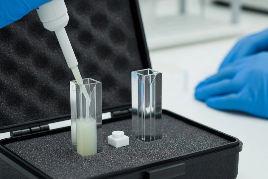
Какие допуски на толщину указывают спектроскопические и аналитические приборы?
Спектроскопия и аналитические приборы полагаются на точные допуски толщины кварцевой пластины для обеспечения точности измерений. Правильный уровень допуска напрямую влияет на точность абсорбции, калибровку и надежность прибора. При выборе правильной спецификации инженеры должны соотнести требования к производительности и производственные затраты.
Стандартные 10-миллиметровые кюветы: ±0,10 мм для рутинной аналитической химии
Стандартные 10-миллиметровые кюветы имеют допуск по толщине ±0,10 мм, что позволяет проводить большинство рутинных лабораторных анализов. Этот допуск позволяет поддерживать погрешность длины пути в пределах ±1%, что соответствует типичному бюджету погрешности при измерении абсорбции в ежедневных химических анализах. Конструкция обеспечивает надежные результаты для качества воды, биохимических и образовательных приложений.
Более жесткий допуск повышает точность измерений, но увеличивает производственные затраты. Например, уменьшение допуска с ±0,10 мм до ±0,05 мм может увеличить стоимость на 20-40%. В следующей таблице показано, как допуск на длину пути влияет на точность измерения абсорбции:
Допуск на длину пути | Влияние на точность абсорбции |
|---|---|
±0,01 мм | Минимальная погрешность измерений |
±0,05 мм | Значительная погрешность в измерениях |
Большинство лабораторий выбирают ±0,10 мм для стандартных кювет, поскольку это позволяет сбалансировать стоимость и производительность для рутинного анализа.
Ячейки с малой длиной пути (1-5 мм): ±0,05 мм для образцов с высокой концентрацией
Ячейки с малой длиной пути, от 1 мм до 5 мм, требуют более жесткого допуска по толщине ±0,05 мм. В таких кюветах измеряются высококонцентрированные образцы, где даже небольшие ошибки длины пути могут привести к значительным погрешностям в расчетах концентрации. Высокоточные кюветы с допуском ±0,01 мм еще больше снижают погрешность измерений, но они имеют более высокую стоимость.
Малая длина пути усиливает влияние ошибок толщины
Ошибка 0,1 мм в ячейке 1 мм приводит к ошибке поглощения 10%
Жесткие допуски обеспечивают надежные результаты при анализе ДНК, белков и микрообъемов
Для достижения этих допусков производители используют передовые методы шлифования и контроля. Лаборатории выбирают подходящий допуск в зависимости от требуемой точности измерения и типа образца.
Сертифицированные эталоны: ±0,02 мм для метрологической прослеживаемости
Сертифицированные эталоны требуют строжайших допусков по толщине, часто достигающих ±0,02 мм. Эти стандарты обеспечивают прослеживаемость измерений абсорбции и поддерживают соответствие нормативным требованиям. Благодаря жестким допускам погрешность длины пути остается ниже 0,2%, что очень важно для калибровки и межлабораторных сравнений.
В следующей таблице приведена зависимость между допуском и точностью измерения:
Уровень толерантности | Ошибка длины пути | Ошибка абсорбции |
|---|---|---|
±0,02 мм | 0.2% | 0.2% |
±0,10 мм | 1% | 1% |
Инженеры выбирают эти сверхточные кюветы для проверки приборов, фармацевтических испытаний и сертифицированной калибровки.
Проточные ячейки и мониторинг процесса: ±0,10-0,15 мм с приоритетом долговечности
В проточных кюветах и приборах для мониторинга процессов используются допуски по толщине от ±0,10 мм до ±0,15 мм. В этих приложениях механическая прочность и химическая стойкость важнее абсолютной точности размеров. Более широкие допуски позволяют создать прочную конструкцию, которая необходима для длительной работы в жестких условиях.
Долговечность и устойчивость к давлению имеют приоритетное значение
Более широкие допуски снижают производственные затраты
Достаточная точность для мониторинга тенденций и промышленного анализа
Инженеры выбирают эти допуски, чтобы обеспечить надежную работу при минимальных затратах. Такой подход обеспечивает долгосрочную эксплуатацию систем мониторинга технологических процессов.
Флуоресценция и специальные приложения: ±0,08 мм с полировкой со всех сторон
Для приложений флуоресценции и специализированной спектроскопии требуется допуск по толщине ±0,08 мм в сочетании с оптической полировкой со всех сторон. Такие требования минимизируют рассеянный свет и фоновую флуоресценцию, которые могут помешать чувствительным измерениям. Использование кварца со сверхнизким уровнем флуоресценции и точных методов полировки обеспечивает высокое соотношение сигнал/шум.
Полировка со всех сторон уменьшает фоновые помехи
Кварц с низким уровнем флуоресценции повышает чувствительность измерений
Жесткие допуски поддерживают передовые исследования и диагностику
Эти характеристики делают компоненты идеальными для спектроскопии флуоресценции, комбинационного рассеяния и кругового дихроизма, где точность измерений имеет решающее значение.
Какие допуски по толщине используются в промышленных высокотемпературных и лабораторных приложениях?
В промышленных и лабораторных условиях часто требуются кварцевые пластины с допусками по толщине, в которых приоритет отдается долговечности и функциональности, а не предельной точности. Такие области применения, как предметные стекла микроскопов, окна печей и реакционные сосуды, имеют уникальные требования к допускам в зависимости от их эксплуатационных требований. Понимание этих требований помогает пользователям выбрать правильную кварцевую пластину, обеспечивающую как производительность, так и экономическую эффективность.
Слайды лабораторного микроскопа: ±0,15 мм для стандартного биологического анализа и анализа материалов
Толщина предметных стекол лабораторных микроскопов обычно составляет ±0,15 мм. Этот допуск позволяет проводить стандартные биологические исследования и анализ материалов, поскольку большинство объективов микроскопов могут компенсировать небольшие изменения толщины за счет регулировки фокуса. Основное внимание уделяется плоскостности поверхности и оптической чистоте, что обеспечивает надежную визуализацию для рутинной лабораторной работы.
Стандарт ISO 8255-1:2017 устанавливает размерные и оптические требования к покровным стеклам для микроскопов. Стандартная толщина для большинства объективов составляет 0,17 мм, а покровные стекла бывают нескольких классов, включая номера 0, 1, 1,5 и 2. Высокопроизводительные покровные стекла могут иметь допуски до ±0,005 мм, что позволяет минимизировать оптические аберрации для объективов с высокой числовой апертурой.
Отклонение от номинальной толщины может вызвать сферическую аберрацию, особенно при получении расширенных изображений. Правильный выбор толщины предметного и покровного стекол обеспечивает оптимальное качество изображения и уменьшает погрешности измерений.
Ключевые моменты:
Стандартные слайды используют допуск ±0,15 мм для рутинного анализа
Стандарты ISO определяют выбор защитного стекла
Объективы с высоким АЧХ требуют более жестких допусков
Правильная толщина минимизирует оптические аберрации
Точные подложки для микроскопии: ±0,05-0,10 мм для количественной визуализации
Подложки для прецизионной микроскопии требуют более жестких допусков по толщине, обычно от ±0,05 мм до ±0,10 мм. Такие подложки поддерживают количественные методы визуализации, такие как фазовый контраст и микроскопия сверхразрешения, где даже небольшие отклонения по толщине могут вносить погрешности в измерения. Для объективов с высокой числовой апертурой часто требуется толщина покровного стекла 0,17 мм ± 0,01 мм для сохранения достоверности изображения.
Производители добиваются таких допусков благодаря современным процессам шлифовки и полировки. Подложки с TTV (общее отклонение толщины) менее 0,015 мм помогают поддерживать равномерную плоскость изображения, что очень важно для получения количественных результатов. Данные стандартов микроскопии показывают, что отклонение всего на 0,01 мм от номинальной толщины может существенно повлиять на сферические аберрации и разрешение.
Тип субстрата | Типичный допуск | Влияние на визуализацию |
|---|---|---|
Стандартный слайд | ±0,15 мм | Достаточно для повседневного использования |
Прецизионная подложка | ±0,05-0,10 мм | Требуется для выполнения количественных работ |
Покрывало с высоким азотом | ±0,005-0,01 мм | Минимизирует аберрации |
Выбор правильной подложки обеспечивает точную визуализацию и достоверные данные для передовых приложений микроскопии.
Окна высокотемпературных печей: ±0,30 мм для визуального наблюдения при 1000-1200°C
Для окон высокотемпературных печей используется допуск по толщине ±0,30 мм. Эти окна должны выдерживать многократные термические циклы при температурах до 1200°C, поэтому механическая прочность и устойчивость к тепловым ударам имеют приоритет над точностью размеров. Более широкий допуск позволяет создать прочную конструкцию и снизить производственные затраты на 40% по сравнению с оптикой с прецизионной шлифовкой.
Для окон печей инженеры выбирают кварцевые пластины толщиной от 5 до 25 мм. Главное требование - чтобы стекло оставалось чистым и неповрежденным на протяжении всего срока службы, даже после сотен циклов нагрева и охлаждения. Данные промышленных стандартов показывают, что допуск ±0,30 мм не влияет на визуальный контроль, но значительно повышает долговечность.
Краткое изложение ключевых моментов:
Допуск ±0,30 мм обеспечивает долговечность при высоких температурах
Механическая прочность и ударопрочность имеют решающее значение
Более широкий допуск снижает производственные затраты
Не влияет на качество визуального наблюдения
Сверхтолстые защитные пластины: ±0,50 мм для экстремальных условий эксплуатации
Сверхтолстые защитные пластины требуют самых больших допусков по толщине, часто ±0,50 мм. Такие пластины используются в экстремальных условиях, таких как плазменная резка, реакторы высокого давления и взрывозащищенные барьеры. Основная функция - обеспечение механической прочности и химической стойкости, а не оптической прозрачности.
Производители выпускают эти плиты толщиной от 50 до 100 мм с допусками, составляющими лишь около 1% от общей толщины. Такой подход позволяет ускорить производство и увеличить выход продукции, что важно для крупномасштабного промышленного использования. Данные по производственным партиям показывают, что уменьшение допуска с ±0,10 мм до ±0,50 мм позволяет снизить затраты более чем на 50%.
Приложение | Типичная толщина | Толерантность | Основное требование |
|---|---|---|---|
Плазменная/лазерная защита | 50-100 мм | ±0,50 мм | Механическая прочность |
Окна высокого давления | 80 мм | ±0,60 мм | Устойчивость к ударам и давлению |
Выбор сверхтолстых пластин со смягченными допусками обеспечивает безопасность и экономическую эффективность в сложных условиях.
Лабораторные реакционные сосуды и ячейки: ±0,20-0,30 мм с учетом химической совместимости
Лабораторные реакционные сосуды и ячейки имеют допуски по толщине от ±0,20 мм до ±0,30 мм. Эти компоненты должны выдерживать воздействие сильных кислот, щелочей и высоких температур, поэтому химическая совместимость и механическая прочность имеют приоритет перед жестким контролем размеров. Толщина стенок большинства сосудов составляет от 2 мм до 10 мм, что обеспечивает необходимую прочность при многократном использовании.
Кварцевые реакционные сосуды сохраняют высокую чистоту и выдерживают резкие изменения температуры. Инженеры указывают более широкие допуски, чтобы снизить затраты и обеспечить надежную работу сосуда в суровых условиях.
Ключевые моменты:
Допуск ±0,20-0,30 мм обеспечивает баланс между прочностью и стоимостью
Химическая стойкость имеет большое значение
Более широкий допуск способствует созданию надежных конструкций судов
Подходит для различных лабораторных применений
Выбор правильного допуска для каждого применения обеспечивает производительность и ценность в промышленных и лабораторных условиях.
Как требования к применению и ограничения по стоимости определяют оптимальный выбор допуска толщины?
Выбор правильного допуска по толщине для кварцевых пластин оптического класса зависит как от технических требований приложения, так и от бюджета проекта. Инженеры должны проанализировать, как изменение толщины влияет на производительность системы, и взвесить влияние более жестких допусков на стоимость. Понимание этих факторов помогает командам избежать ненужных расходов и при этом соответствовать функциональным требованиям.
Анализ функциональных требований: определение минимально допустимых отклонений
Инженеры начинают с определения ключевых параметров производительности для каждого приложения. Они используют такие методы измерения, как LVDTдля мониторинга в реальном времени в промышленных условиях, оптические системы для высокоточной оптики и емкостные датчики для тонких пленок. Каждый метод обладает уникальными преимуществами, помогая инженерам подобрать допуск в соответствии с реальными требованиями к производительности.
Метод измерения | Контекст приложения | Преимущества |
|---|---|---|
LVDTs | Промышленный контроль толщины | Высокая точность, экономичность |
Оптические системы | Прецизионные оптические компоненты | Чувствительный, идеально подходит для высокоточных приложений |
Емкостные датчики | Измерение тонких пленок | Чрезвычайно точный |
Индуктивные датчики | Бесконтактное измерение металла | Компактный, устойчивый к загрязнениям |
Типичные допуски для оптических компонентов составляют от ±0,20 мм для стандартного качества до ±0,010 мм для высокой точности. Завышение допусков может привести к увеличению затратЭто увеличивает время выполнения заказа и повышает процент брака. Многие оптические системы допускают регулировку, компенсирующую незначительные погрешности, поэтому не для каждой детали требуется самый строгий допуск.
Ключевые моменты, которые необходимо учитывать:
Проанализируйте, как толщина влияет на производительность
Выберите самый широкий допуск, соответствующий требованиям
Избегайте завышения спецификации, чтобы контролировать расходы и сроки выполнения заказа
Проверка возможностей поставщика и протоколы обеспечения качества
Проверка возможностей поставщика гарантирует, что кварцевые пластины соответствуют заданным допускам и стандартам качества. Ведущие поставщики проходят сертификацию по стандарту ISO 9001:2015, предоставляют прослеживаемую документацию о соответствии и согласовывают проверку качества с потребностями заказчика. Кроме того, они обеспечивают изготовление деталей нестандартных размеров и допуски точности до ±0,05 мм для высокоточных деталей.
Мера обеспечения качества | Описание |
|---|---|
Сертифицировано по стандарту ISO 9001:2015 | Обеспечивает стабильное качество продукции |
Прослеживаемая документация по соответствию | Гарантирует прослеживаемость материалов |
Подтверждение качества, ориентированное на клиента | Соответствие валидации требованиям клиента |
Допуски | Точность до ±0,05 мм для отдельных компонентов |
Протоколы обеспечения качества включают сертификаты соответствия, отчеты об испытаниях материалов и отчеты о проверке размеров. Проверки качества в процессе производства и аудиты поставщиков рекомендуются для критически важных приложений. Требование строгой документации по контролю качества помогает поддерживать надежность и прослеживаемость.
Резюме лучших практик:
Запросите подробную документацию по контролю качества
Узнайте о проверке качества в процессе производства
Проведение аудита поставщиков критически важных деталей
Следуя этим шагам, инженеры смогут с уверенностью выбрать кварцевые пластины, обеспечивающие баланс между производительностью, качеством и стоимостью.
Выбор правильных допусков на толщину кварцевых пластин оптического качества зависит от области применения. В таблице ниже приведены типичные допуски и справочные данные:
Тип пластины | Допуск по толщине | Стандартная ссылка |
|---|---|---|
Печная плита | ±0,5 мм | ISO 9050 |
Аналитическое окно | ±0,10 мм | ISO 9050 |
Прецизионная оптика | ±0,05 мм | ISO 9050 |
Соответствие допусков потребностям приложений повышает производительность и снижает затраты.
Для достижения наилучших результатов инженерам следует ознакомиться с отраслевыми стандартами и работать с квалифицированными поставщиками.
ЧАСТО ЗАДАВАЕМЫЕ ВОПРОСЫ
Каков наиболее распространенный допуск по толщине для кварцевых пластин оптического класса?
Производители обычно указывают ±0,10 мм для стандартных кварцевых пластин оптического качества. Этот допуск отвечает большинству лабораторных и промышленных потребностей. Инженеры выбирают более жесткие допуски для высокоточных приложений.
Какие факторы определяют необходимый допуск по толщине?
Инженеры учитывают тип применения, требования к производительности и ограничения по стоимости. Оптические системы требуют более жестких допусков для обеспечения точности. Для промышленного применения приоритетны долговечность и стоимость.
Совет: Для достижения наилучших результатов всегда подбирайте допуск в соответствии с функциональными потребностями.
Что произойдет, если допуск окажется слишком жестким для конкретной задачи?
Излишне жесткие допуски увеличивают производственные затраты и время выполнения заказа. Большинство систем не выигрывают от повышенной точности. Инженеры должны избегать завышения допусков.
Уровень толерантности | Влияние на стоимость | Время выполнения |
|---|---|---|
Стандарт | Низкий | Короткие |
Сверхточный | Высокий | Длинный |
Какими мерами контроля качества проверяется допуск по толщине?
Поставщики используют калиброванные измерительные инструменты, сертификаты ISO и отчеты о проверках. Инженеры запрашивают сертификаты соответствия и данные испытаний материалов для критически важных деталей.
Ключевые моменты:
Сертифицированные измерения обеспечивают точность
Документация поддерживает прослеживаемость
Регулярные аудиты поддерживают качество
Что такое общая вариация толщины (TTV) и почему она имеет значение?
Общая вариация толщины (TTV) измеряет разницу между самой толстой и самой тонкой точками пластины. Низкий показатель TTV улучшает однородность в оптических и термических приложениях.
Низкий уровень TTV: Лучшая производительность
Высокий уровень TTV: Риск неравномерного нагрева или оптических искажений