- Accueil
- /
- Applications
- /
- Semi-conducteur Verre de quartz
- /
- Gravure sur quartz à processus optimisé...


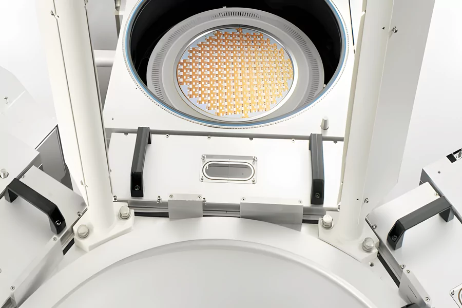
Anneaux de gravure en quartz optimisés pour les chambres à plasma pour semi-conducteurs-TOQUARTZ®.
Caractéristiques de l'anneau de gravure en quartz
Les anneaux de quartz TOQUARTZ® pour semi-conducteurs sont conçus spécifiquement pour les équipements de gravure au plasma, offrant des propriétés exceptionnelles qui garantissent des conditions de processus stables et une durée de vie prolongée dans les environnements de fabrication de semi-conducteurs exigeants.
Pureté des matériaux
Fabriqué à partir de quartz de première qualité d'une pureté de 99,99% SiO₂ (jusqu'à 99,995% disponible), il minimise la contamination potentielle dans les processus critiques des semi-conducteurs.
Stabilité thermique
Résiste à des températures extrêmes allant jusqu'à 1600°C avec une dilatation thermique minimale (coefficient : 0,5×10-⁶/K), ce qui garantit la stabilité dimensionnelle pendant les cycles thermiques dans les processus de gravure au plasma.
Compatibilité des processus
Conçue spécifiquement pour les procédés de gravure des semi-conducteurs, y compris les systèmes ICP, RIE et DRIE, avec des dimensions optimisées pour diverses configurations de chambres.
- Résiste aux produits de gravure des semi-conducteurs
- Coefficient de frottement extrêmement faible
- Assure une bonne étanchéité de la chambre de gravure
Spécifications techniques et dimensions de l'anneau de gravure en quartz
Les anneaux de gravure en quartz TOQUARTZ® sont fabriqués selon les spécifications précises requises pour les équipements de traitement des semi-conducteurs, et présentent des propriétés physiques, chimiques et thermiques contrôlées.
Spécifications techniques de l'anneau de gravure en quartz
| Propriété | Valeur | Notes |
| Matériau | Quartz de haute pureté | 99.99% SiO₂ standard (jusqu'à 99.995% disponible) |
| Densité | 2,2 g/cm³ | ±0,02 g/cm³ |
| Résistance à la flexion | 48 MPa | A température ambiante |
| Module d'élasticité | 72 GPa | Module d'Young |
| Rapport de Poisson | 0.14-0.17 | – |
| Résistance à la compression | 1100 MPa | A température ambiante |
| Dureté Moh's | 5.5-6.5 | – |
| Température de fonctionnement maximale (à long terme) | 1100°C | Fonctionnement continu |
| Température de fonctionnement maximale (à court terme) | 1350°C | Exposition intermittente |
| Conductivité thermique | 1,4 W/m-K | A 20°C |
| Coefficient de dilatation thermique | 5.5×10-⁷/°C | Gamme 20-1000°C |
| Résistance spécifique | 7×10⁷ Ω-cm | A 20°C |
| Rugosité de surface | Ra≤0.8μm | Finition standard |
Tableau des tailles de l'anneau en quartz fondu gravé
| Modèle | Spécifications | Diamètre extérieur (mm) | Épaisseur (mm) | Pureté (%) |
| AT-TAZ-ER001 | 2 pouces | 50.8 | 3 | 99.99 |
| AT-TAZ-ER002 | 4 pouces | 101.6 | 4 | 99.99 |
TOQUARTZ® relève les défis de la gravure des semi-conducteurs
avec anneaux de quartz
Anneaux de gravure au quartz dans les usines de semi-conducteurs à haut volume : Prévenir les arrêts coûteux de la chaîne de production
Principaux avantages
-
Soutien au programme de remplacement programmé
TOQUARTZ prend en charge les livraisons à cycle fixe alignées sur les fenêtres de maintenance de 3 à 6 mois. -
Exécution d'urgence en <48 heures
Les anneaux de gravure sur quartz standard peuvent être expédiés dans le monde entier dans les 48 heures afin d'éviter les temps d'arrêt. -
Taux de cohérence des lots ≥ 99,7%
L'uniformité des dimensions et des matériaux d'un lot à l'autre garantit qu'il n'y a pas de défaillance imprévue.
Solution TOQUARTZ
Une usine américaine de DRAM de 12 pouces fonctionnant 24 heures sur 24 et 7 jours sur 7 a enregistré des pertes de $220 000 euros par jour en raison de défaillances imprévues de l'anneau de gravure.
TOQUARTZ® a mis en place un plan de réapprovisionnement sur 90 jours et un stock tampon d'urgence.
En l'espace de six mois, les incidents liés aux temps d'arrêt ont diminué de 83% et les interruptions de processus liées aux anneaux ont été éliminées.
L'usine maintient maintenant un taux de disponibilité de 99,9% dans son module de gravure avec TOQUARTZ comme seul fournisseur d'anneaux.
Anneaux de gravure en quartz fondu pour les fabricants d'équipements sur mesure : Répondre à des exigences dimensionnelles précises
Principaux avantages
-
±0,08mm Tolérance sur OD/ID
TOQUARTZ atteint une tolérance de ±0,08 mm sur les diamètres extérieur/intérieur pour les conceptions de chambres spécifiques aux OEM. -
Précision de la position du trou ≤ ±0,1mm
Les trous de montage sont percés par CNC avec un écart de position ≤ ±0,1 mm sur une portée de 100 mm. -
Écart d'un lot à l'autre < 0,05 mm
Les écarts dimensionnels entre les lots sont inférieurs à 0,05 mm pour garantir la répétabilité de l'assemblage.
Solution TOQUARTZ
Un équipementier allemand avait besoin d'anneaux de quartz de 6 pouces avec 6 trous de montage asymétriques et une tolérance de ±0,1 mm.
Les fournisseurs précédents avaient un taux de rejet de 12% en raison du mauvais alignement des trous et de l'écaillage des bords.
TOQUARTZ® a livré 300 anneaux avec un rejet de 0% et une déviation de <0,03 mm vérifiée par des rapports de MMT.
L'équipementier a réduit le temps de reprise de l'assemblage de 40% et a signé un contrat d'approvisionnement de deux ans.
Anneaux de gravure en verre quartz pour le développement de procédés avancés : Exigences en matière de pureté des matériaux
Principaux avantages
-
Impureté métallique ≤ 10ppb
Les anneaux de quartz TOQUARTZ sont certifiés avec ≤10ppb d'impuretés métalliques totales pour la recherche et le développement de nœuds avancés. -
CF₄/O₂ Endurance plasmatique ≥ 72h
Les anneaux conservent leur intégrité structurelle après une exposition de 72 heures au plasma CF₄/O₂ à 800°C. -
Nombre de particules en surface < 5 pcs/cm².
Le nombre de particules après le nettoyage est contrôlé en dessous de 5 pcs/cm² (≥0,3μm) dans des conditions ISO de classe 5.
Solution TOQUARTZ
Un laboratoire japonais de R&D développant des nœuds logiques de 3 nm avait besoin d'anneaux de quartz ultra-purs pour la gravure à base de CF₄.
TOQUARTZ® a fourni des anneaux avec une teneur en métal ≤8ppb et des particules de surface <3 pcs/cm².
Après 72 heures d'exposition au plasma, aucune dégradation structurelle ou contamination n'a été détectée.
Le laboratoire a constaté une réduction de 92% des défauts induits par les particules par rapport aux fournisseurs précédents.
Services de personnalisation TOQUARTZ® pour les bagues de gravure sur quartz
Capacités de conception sur mesure
-
Personnalisation dimensionnelle
Diamètres extérieurs/intérieurs, épaisseurs et profils des bords sur mesure, adaptés à la conception spécifique de votre chambre. -
Caractéristiques de montage
Trous de montage percés avec précision, fentes, encoches ou autres caractéristiques pour assurer un alignement et une installation corrects. -
Caractéristiques de montage
Trous de montage percés avec précision, fentes, encoches ou autres caractéristiques pour assurer un alignement et une installation corrects. -
Traitements de surface
Finitions de surface spéciales, y compris le polissage au feu, le meulage ou le nettoyage chimique pour répondre à des exigences spécifiques en matière de rugosité de surface.
Processus de commande personnalisé
-
Analyse des besoins
Soumettez des dessins, des spécifications ou des échantillons. Nos ingénieurs examineront et discuteront des exigences techniques. -
Confirmation de la conception
Nous fournissons des dessins détaillés pour approbation avant le début de la production. -
Développement de prototypes
Pour les conceptions complexes, nous pouvons produire des prototypes à des fins d'essai et de validation. -
Production et contrôle de la qualité
Des inspections et des tests rigoureux garantissent que toutes les spécifications sont respectées. -
Livraison et soutien
Livraison rapide avec documentation complète et support technique.
Conseils d'utilisation et d'entretien de l'anneau de gravure en quartz
La manipulation, l'installation et l'entretien corrects des anneaux de traitement en quartz sont essentiels pour maximiser les performances et la durée de vie dans les applications de gravure des semi-conducteurs.
Manutention et installation
- Manipulez toujours les anneaux de quartz avec des gants de salle blanche non poudrés afin d'éviter toute contamination.
- Vérifier qu'il n'y a pas d'éclats, de fissures ou de défauts de surface avant l'installation.
- S'assurer que les surfaces de montage sont propres et exemptes de particules
- Serrer progressivement le matériel de montage en croix pour assurer une répartition uniforme de la pression.
- Éviter le serrage excessif qui peut créer des points de tension et entraîner des fractures.
- Ne jamais utiliser d'outils métalliques directement sur les surfaces en quartz pendant l'installation.
Entretien et remplacement
- Établir un calendrier d'inspection régulier en fonction des conditions du processus
- Surveiller les signes d'érosion, de décoloration ou de changements dimensionnels.
- Intervalle de remplacement typique : 500-1000 heures de fonctionnement (varie selon l'application)
- Élaborer un calendrier de remplacement proactif afin d'éviter les temps d'arrêt non planifiés
- Nettoyer en utilisant uniquement des solvants approuvés pour les semi-conducteurs si nécessaire.
- Éviter les changements brusques de température qui peuvent provoquer un choc thermique
Recommandations en matière de stockage
- Conserver dans l'emballage d'origine jusqu'au moment de l'utilisation
- Maintenir dans un environnement propre et sec avec une humidité contrôlée
- Conditions de stockage idéales : 20-25°C, 40-60% humidité relative
- Utilisez des matériaux doux et non pelucheux pour séparer les différents anneaux.
- Évitez d'empiler des objets lourds sur les composants en quartz.
Besoin d'une assistance technique pour les anneaux de gravure à quartz ?
Pourquoi s'associer à TOQUARTZ ?
Avantage de l'usine directe
En tant que fabricant direct, nous pouvons supprimer les nombreux liens intermédiaires.
Expertise en ingénierie
L'équipe technique guide les clients depuis la sélection des matériaux jusqu'à l'optimisation de la conception, en traduisant les spécifications en produits livrables.
Fabrication flexible
Traiter les commandes standard et personnalisées grâce à une expertise en matière de petites séries et à une rigueur de prototypage afin de respecter les délais urgents.
Qualité
Assurance
Validation en 3 étapes avant expédition :
1. la précision des dimensions,
2. pureté du matériau ,
3. les seuils de performance
Chaîne d'approvisionnement mondiale
Logistique mondiale fiable vers les centres industriels (DE/US/JP/KR en priorité) avec des étapes traçables.
Produits réimprégnés
En tant que fabricant spécialisé disposant de capacités d'usinage directes, TOQUARTZ fournit des solutions en quartz standard et personnalisées avec une assistance technique tout au long du processus de spécification et de mise en œuvre.
FAQ
Q : À quoi sert un anneau de gravure en quartz dans la fabrication des semi-conducteurs ?
R : Les anneaux de gravure en quartz (également appelés anneaux de traitement en quartz) sont des composants essentiels de l'équipement de gravure au plasma utilisé dans la fabrication des semi-conducteurs. Ils servent d'espaceurs entre la chambre à plasma et le substrat à graver, contribuant à contenir et à diriger le plasma, à maintenir l'uniformité du processus et à prévenir la contamination. Leur grande pureté, leur stabilité thermique et leur résistance chimique les rendent idéaux pour résister aux environnements plasmatiques agressifs utilisés dans les processus de gravure des plaquettes.
Q : Comment un anneau de quartz améliore-t-il les processus de gravure au plasma ?
R : Les anneaux de quartz améliorent les processus de gravure au plasma de plusieurs façons :
(1) Ils contribuent à maintenir un environnement plasma homogène en assurant un espacement et un alignement précis à l'intérieur de la chambre,
(2) Leur grande pureté empêche la contamination métallique qui pourrait compromettre les performances des dispositifs semi-conducteurs,
(3) Leur stabilité thermique garantit la constance des dimensions lors des fluctuations de température ;
(4) Leurs propriétés d'isolation électrique permettent de contrôler la distribution du plasma.
Ces avantages contribuent collectivement à améliorer l'uniformité de la gravure, à augmenter le rendement des processus et à améliorer la cohérence des performances des dispositifs.
Q : Quelles sont les exigences en matière de matériaux pour les anneaux de quartz utilisés dans la gravure des semi-conducteurs ?
R : Les anneaux de quartz destinés à la gravure des semi-conducteurs doivent répondre à des exigences strictes en matière de matériaux :
(1) Haute pureté (généralement 99,99% SiO₂ ou plus) pour éviter toute contamination,
(2) Excellente stabilité thermique permettant de supporter des températures de traitement allant jusqu'à 1600°C,
(3) Résistance chimique supérieure aux gaz corrosifs et au plasma,
(4) Faible coefficient de dilatation thermique pour la stabilité dimensionnelle,
(5) Propriétés constantes du matériau avec un minimum de défauts ou d'inclusions,
(6) Tolérances dimensionnelles précises, typiquement ±0,1 mm ou mieux.
Ces exigences garantissent la fiabilité du processus et évitent les pertes de rendement dans la fabrication des plaquettes.
Q : Vos bagues en quartz sont-elles compatibles avec les procédés de gravure à base de fluor ?
R : Oui, nos anneaux de gravure en quartz sont compatibles avec les procédés de gravure à base de fluor couramment utilisés dans la fabrication des semi-conducteurs. Notre formulation de quartz de haute pureté offre une excellente résistance aux gaz fluorés tels que CF₄, SF₆, NF₃ et CHF₃. Alors que tous les quartz subissent une érosion progressive dans les environnements de plasma de fluor, les anneaux TOQUARTZ font preuve d'une durabilité supérieure avec des taux d'érosion typiquement 20-30% inférieurs à ceux du quartz commercial standard. Pour les procédés au fluor particulièrement agressifs, nous pouvons recommander des compositions et des épaisseurs optimisées afin de maximiser la durée de vie.
Q : Comment les bagues de gravure en quartz se comparent-elles aux bagues en céramique ?
R : Les anneaux de gravure en quartz et les alternatives en céramique (généralement l'alumine ou le nitrure d'aluminium) présentent chacun des avantages distincts : Le quartz offre une pureté supérieure (99,99%+ SiO₂), une excellente transparence pour le contrôle optique, une faible génération de particules et une très faible dilatation thermique. Les céramiques offrent généralement une meilleure résistance mécanique, une conductivité thermique plus élevée et, dans certains cas, une meilleure résistance à des chimies de plasma spécifiques. Le choix dépend des exigences du processus - le quartz est généralement préféré pour les applications nécessitant une grande pureté, une clarté optique et une dilatation thermique minimale, tandis que les céramiques peuvent être sélectionnées pour les applications nécessitant une plus grande résistance structurelle ou une meilleure gestion thermique.
Contactez notre équipe d'ingénieurs pour une consultation technique et un devis. Nous vous aiderons à sélectionner les spécifications optimales pour votre application.